Supercharge Your Innovation With Domain-Expert AI Agents!

Nonvolatile memory device and method of testing the same

a technology of nonvolatile memory and test method, which is applied in the direction of static storage, digital storage, instruments, etc., can solve the problems of inefficient time and production cos

Inactive Publication Date: 2012-04-17
SK HYNIX INC
View PDF5 Cites 7 Cited by
  • Summary
  • Abstract
  • Description
  • Claims
  • Application Information

AI Technical Summary

Benefits of technology

Enables efficient and cost-effective self-testing within the memory device, reducing the reliance on external resources and improving production efficiency by allowing internal detection of fail memory cells without external apparatus.

Problems solved by technology

Such a test method may be problematic in that it uses lots of resources, such as a host and coupling equipment, and is inefficient in terms of time and the cost of production because a memory device has to be coupled to an external host.

Method used


Image

  • Nonvolatile memory device and method of testing the same
  • Nonvolatile memory device and method of testing the same
  • Nonvolatile memory device and method of testing the same

Examples


Embodiment Construction

[0029]Hereinafter, some embodiments of the present disclosure will be described in detail with reference to the accompanying drawings. The figures are provided to allow those having ordinary skill in the art to understand the scope of the embodiments of the disclosure.

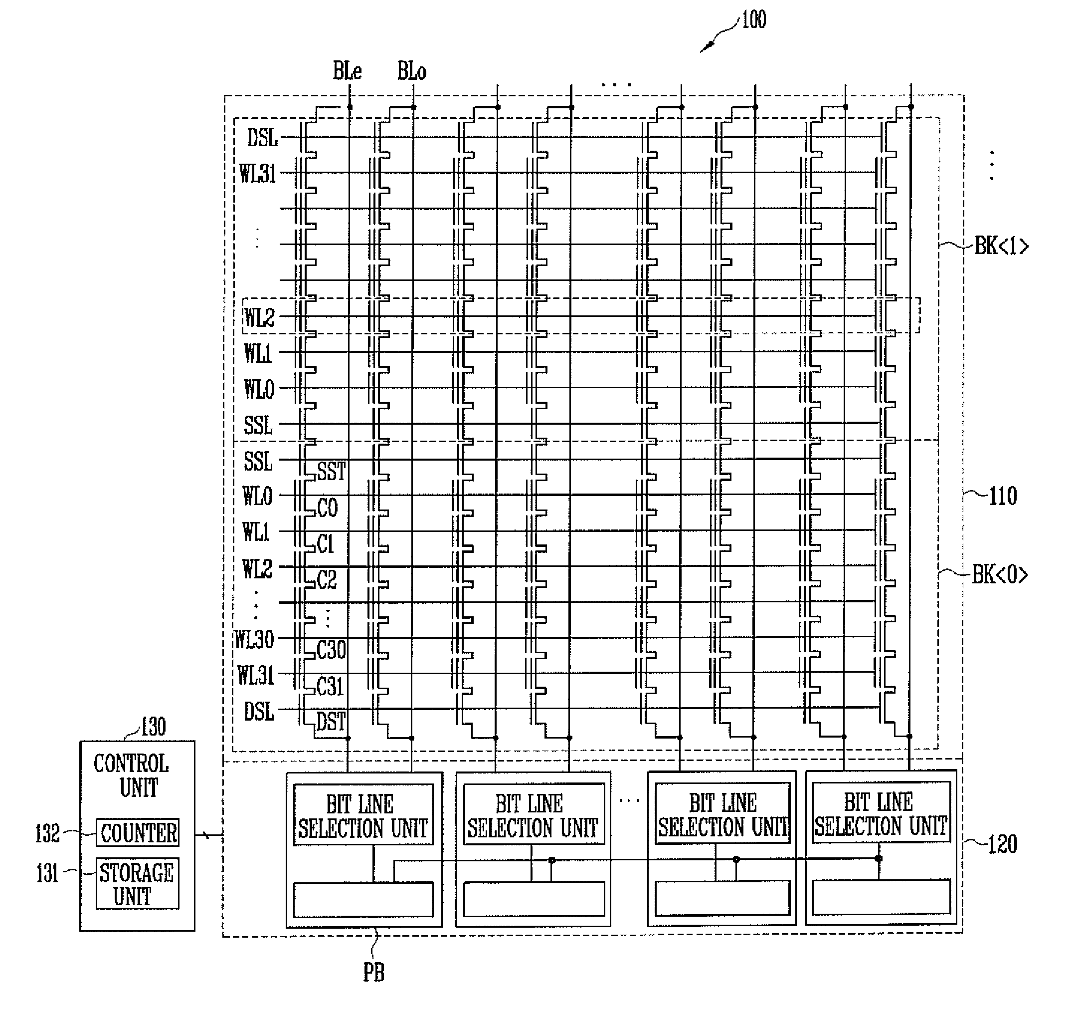
[0030]FIG. 1 is a block diagram of a nonvolatile memory device according to an embodiment of this disclosure.

[0031]Referring to FIG. 1, the nonvolatile memory device 100 includes a memory cell array 110, a page buffer unit 120, and a control unit 130.

[0032]The memory cell array 110 includes a number of memory blocks BK (although FIG. 1 only shows first and second memory blocks BK and BK).

[0033]Each of the memory blocks BK includes a number of cell strings coupled to respective bit lines. Each of the cell strings includes 0th to thirty-first memory cells C0 to C31 coupled in series between a drain select transistor DST and a source select transistor SST.

[0034]0th to thirty-first word lines WL0 to WL31 are respectively c...


PUM


Abstract

A nonvolatile memory device includes a storage unit configured to store pattern data selected based on a test command set, and a control unit configured to consecutively perform a program operation on a number of pages in response to the pattern data to obtain programmed pages, consecutively perform a read operation on the programmed pages, and provide information about a bit line coupled to a fail memory cell and about a number of fail bit lines checked as a result of the read operation.

Description

CROSS-REFERENCE TO RELATED APPLICATION[0001]Priority to Korean patent application number 10-2009-0041672 filed on May 13, 2009, the entire disclosure of which is incorporated by reference herein, is claimed.BACKGROUND[0002]Exemplary embodiments relate to a nonvolatile memory device and, more particularly, to a nonvolatile memory device configured to have an algorithm and pattern data for a self-test built therein, and a method of testing the same.[0003]A nonvolatile memory device may have the advantages of random access memory (RAM), such as enabling the writing and erasure of data, and read only memory (ROM), such as retaining data even without the supply of power, and so has recently been widely used for the storage media of portable electronic devices, such as digital cameras, personal digital assistants (PDAs), and MP3 players.[0004]The nonvolatile memory device may include a memory cell array, a row decoder, a page buffer unit, etc. The memory cell array may include a plurality...

Claims


Application Information

Patent Timeline
Patent Type & Authority Patents(United States)
IPC IPC(8): G11C29/00
CPCG11C29/44G11C29/4401G11C16/04G11C29/72G11C16/10G11C16/26G11C29/025G11C2029/3602
Inventor KANG, TAI KYU
Owner SK HYNIX INC
Features
  • R&D
  • Intellectual Property
  • Life Sciences
  • Materials
  • Tech Scout
  • Unparalleled Data Quality
  • Higher Quality Content
  • 60% Fewer Hallucinations
Learn More