Semiconductor device

a semiconductor device and semiconductor technology, applied in the field of semiconductor devices, can solve the problems of deterioration or destruction of large burden placed on easy deterioration of elements inside the rf tag, so as to prevent deterioration or destruction of elements of semiconductor devices, reduce the distance between the reader/writer and the semiconductor device, and reduce the power supply from the antenna circuit.

Active Publication Date: 2012-04-17
SEMICON ENERGY LAB CO LTD
View PDF52 Cites 26 Cited by
  • Summary
  • Abstract
  • Description
  • Claims
  • Application Information

AI Technical Summary

Benefits of technology

[0009]For example, in the case where the communication distance is very short when a reader / writer and an RF tag are in contact with each other or in the case where the distance between the reader / writer and the RF tag is sharply reduced, the RF tag receives enormous power. In particular, when high power is supplied to an RF tag with the use of a semiconductor integrated circuit formed of a transistor which is driven at a low voltage, deterioration of an element characteristic or destruction of the element easily occurs.
[0011]As an effective measure to prevent deterioration of an element characteristic or destruction of the element due to application of high power, there is a method for connecting a fuse to an input terminal of a semiconductor device; however, in the case where a circuit operates with low power consumption, such as an RF tag, power is largely lost; therefore, the circuit is not adopted so much.
[0012]In view of the foregoing problem, an object of the present invention is to provide a semiconductor device which can prevent deterioration of an element characteristic or destruction of the element, suppress power loss, and communicate in a wide range, even in the case where the communication distance is very short or the case where distance between a reader / writer and an RF tag is sharply reduced.
[0013]Further, an object of the present invention is to provide a semiconductor device which can prevent deterioration of an element characteristic or destruction of the element, suppress power loss, and communicate in a wide range, even in the case where the communication distance is very short or the case where distance between a reader / writer and an RF tag is sharply reduced.
[0019]By use of the present invention, in the case where the communication distance is very short such as the case where the reader / writer and the semiconductor device are in contact with each other, or the case where distance between the reader / writer and the semiconductor device is sharply reduced, power supply from the antenna circuit can be limited, and deterioration or destruction of an element of a semiconductor device can be prevented. Therefore, stable communication can be performed in the semiconductor device, and reliability can be improved. Furthermore, since stable power supply voltage can be supplied from a built-in battery, the semiconductor device can operate normally while power supply from the antenna circuit is limited.

Problems solved by technology

However, as described in Reference 1, in a method for changing a Q value by use of a variable resistance circuit which is connected in parallel to an antenna circuit between input terminals, in the case of short communication distance, signals transmitted from an RF tag are made to be easily read by supplying a large current to an element; therefore, there is a problem in that a large burden is placed on an element inside the RF tag.
In particular, when high power is supplied to an RF tag with the use of a semiconductor integrated circuit formed of a transistor which is driven at a low voltage, deterioration of an element characteristic or destruction of the element easily occurs.
The RF tag receives high power, so that deterioration of an element characteristic or destruction of the element inside the RF tag occurs.
As a result, a circuit inside the RF tag does not function normally and malfunction occurs in some cases.
In the worst case, the circuit inside the RF tag could not operate.
As an effective measure to prevent deterioration of an element characteristic or destruction of the element due to application of high power, there is a method for connecting a fuse to an input terminal of a semiconductor device; however, in the case where a circuit operates with low power consumption, such as an RF tag, power is largely lost; therefore, the circuit is not adopted so much.

Method used


Image

  • Semiconductor device
  • Semiconductor device
  • Semiconductor device

Examples


embodiment 1

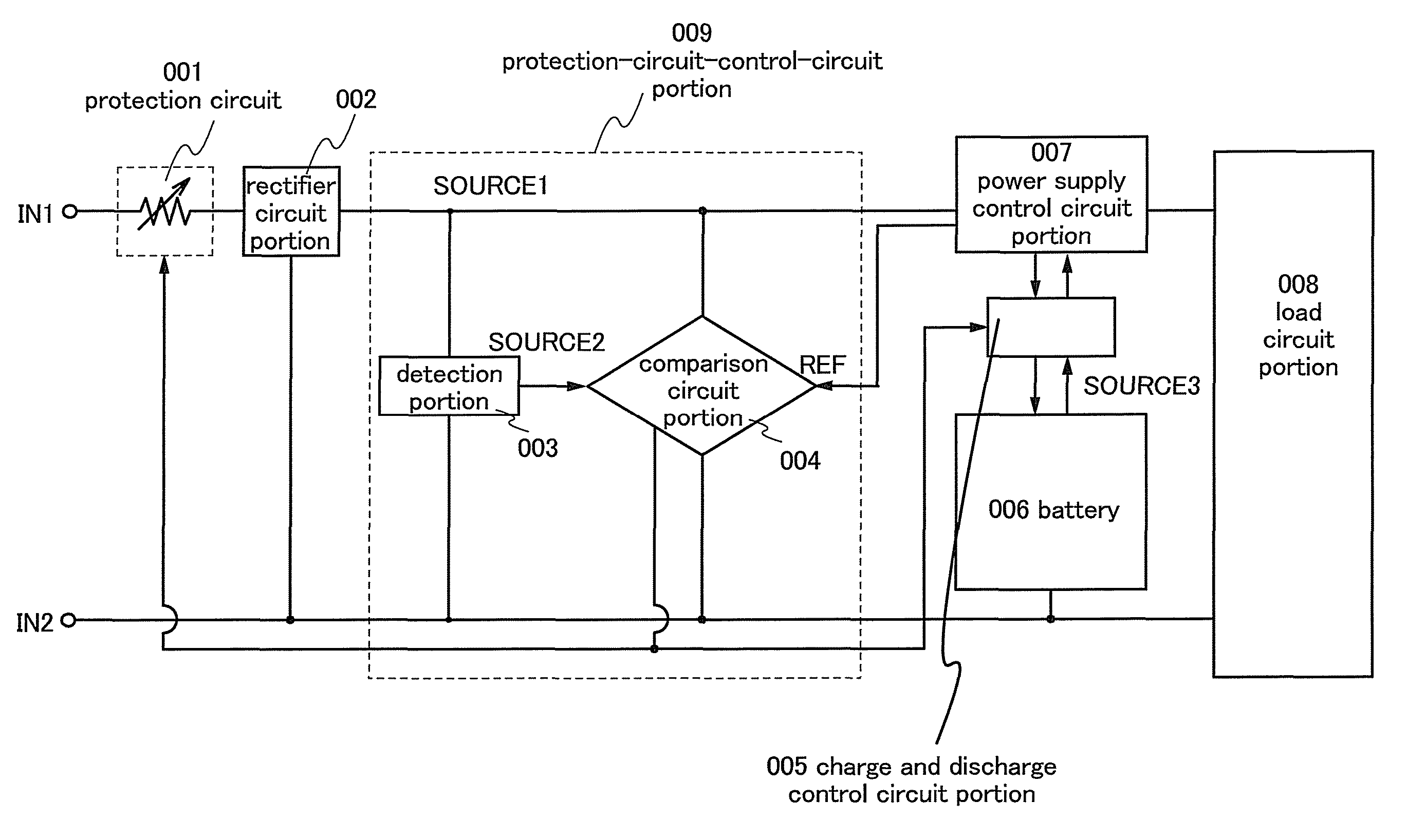
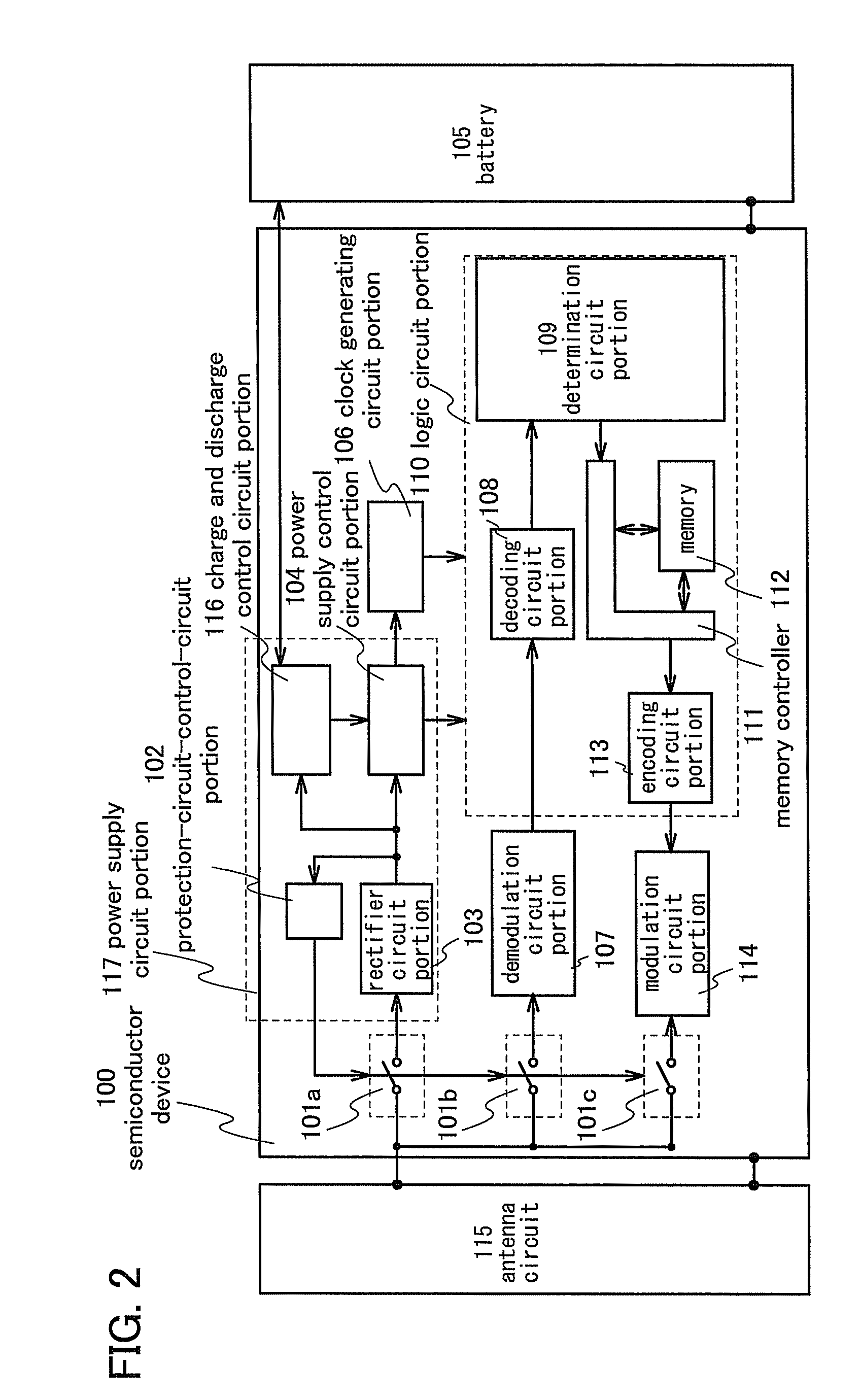
[0058]Next, a structure of a semiconductor device of the present invention will be described with reference to FIG. 2.

[0059]An antenna circuit 115 for communicating with a reader / writer wirelessly is connected to a semiconductor device 100. In this embodiment, a structure of a semiconductor device without including an antenna circuit is described; however, a semiconductor device may include an antenna circuit in its structure.

[0060]The semiconductor device 100 of this embodiment includes protection circuits 101a to 101c each using a variable resistance element which normally has high conductivity and can change a resistance value in accordance with an electrical signal; a power supply circuit portion 117; a logic circuit portion 110; a clock generating circuit portion 106 for generating a clock which is supplied to the logic circuit portion 110; a demodulation circuit portion 107 for demodulating wireless communication data from a reader / writer received by the antenna circuit 115; a...

embodiment 2

[0100]In this embodiment, a method for controlling the resistance value of the variable resistance element included in the protection circuit of the semiconductor device described in Embodiment 1 will be described with reference to FIG. 13. FIG. 13 shows the protection circuit 101a, the protection-circuit-control-circuit portion 102, the rectifier circuit portion 103, and the power supply control circuit portion 104 of the semiconductor device 100 in Embodiment 1, and particularly shows an example of a specific circuit structure of the protection circuit 101a and the protection-circuit-control-circuit portion 102.

[0101]In FIG. 13, the protection circuit 101a includes protection circuits 1301a to 1301c. In this embodiment, an example in which three protection circuits are connected is described; however, the present invention is not limited thereto, and given number of protection circuits can be provided.

[0102]The protection circuit 1301a in FIG. 13 includes a transistor 1302a and a ...

embodiment 3

[0123]In this embodiment, an example of a manufacturing method of the semiconductor device described in Embodiment 1 will be described with reference to the drawings. In this embodiment, a structure in which an antenna circuit and a semiconductor device are provided over the same substrate will be described. Note that the antenna circuit and the semiconductor device can be formed over one substrate and thin film transistors as transistors included in the semiconductor device can be made, so that miniaturization can be achieved.

[0124]First, as shown in FIG. 5A, a separation layer 1903 is formed over a surface of a substrate 1901 with an insulating film 1902 interposed therebetween. Next, an insulating film 1904 which serves as a base film and a semiconductor film 1905 (e.g., a film which includes amorphous silicon) are stacked. Note that the insulating film 1902, the separation layer 1903, the insulating film 1904, and the semiconductor film 1905 can be formed in succession.

[0125]Fur...


PUM


Abstract

A semiconductor device is provided, which comprises a first circuit including a variable resistance element, a second circuit electrically connected to the first circuit, and an antenna circuit configured to supply power to the first circuit. A resistance value of the variable resistance element is changed in accordance with the power supplied from the antenna circuit, and the variable resistance element is electrically connected in series between the second circuit and the antenna circuit.

Description

BACKGROUND OF THE INVENTION[0001]1. Field of the Invention[0002]The present invention relates to a semiconductor device which transmits and receives data by wireless communication. Further, the present invention relates to a semiconductor device which can prevent deterioration of element characteristics and destruction of the element of the semiconductor device in the case where the semiconductor device receives high power in wireless communication.[0003]2. Description of the Related Art[0004]In recent years, research and development on increasing power supply efficiency from a reader / writer to an RF tag has been actively conducted in order to expand a response range in wireless communication system.[0005]In general, power decays in proportion to square of distance from a spot where power is emitted to an observation spot. That is, power to be applied to an RF tag is high as distance (hereinafter referred to as communication distance) between a reader / writer and the RF tag is short,...

Claims


Application Information

Patent Timeline
Patent Type & Authority Patents(United States)
IPC IPC(8): H04B5/00H04B7/00H04B1/38H04B1/28H01L21/822H01L27/04
CPCG06K19/0701G06K19/0715G06K19/0723G08B13/2417
Inventor TADOKORO, ASAMI
Owner SEMICON ENERGY LAB CO LTD
Why Eureka
Try Eureka