Nonvolatile semiconductor memory device and method for manufacturing same

a semiconductor and memory device technology, applied in semiconductor devices, digital storage, instruments, etc., can solve the problems of increasing cost, increasing cost, and unable to reduce costs in recent years, and reducing costs in the field of nonvolatile semiconductor memory devices

Inactive Publication Date: 2012-05-15
KK TOSHIBA
View PDF76 Cites 158 Cited by
  • Summary
  • Abstract
  • Description
  • Claims
  • Application Information

AI Technical Summary

Problems solved by technology

Although the dimensions of one element are reduced (downscaled) to increase the memory capacity of the memory, such downscaling in recent years has become difficult in regard to both cost and technology.
Therefore, costs cannot be reduced even when three dimensional; and instead, stacking four or more layers undesirably leads to cost increases.

Method used


Image

  • Nonvolatile semiconductor memory device and method for manufacturing same
  • Nonvolatile semiconductor memory device and method for manufacturing same
  • Nonvolatile semiconductor memory device and method for manufacturing same

Examples


first embodiment

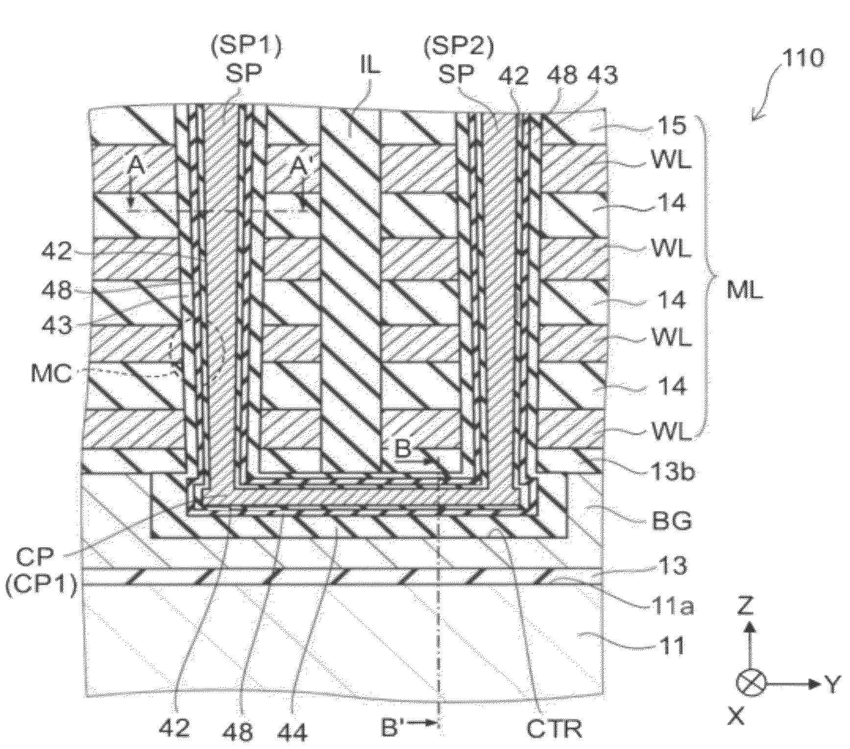
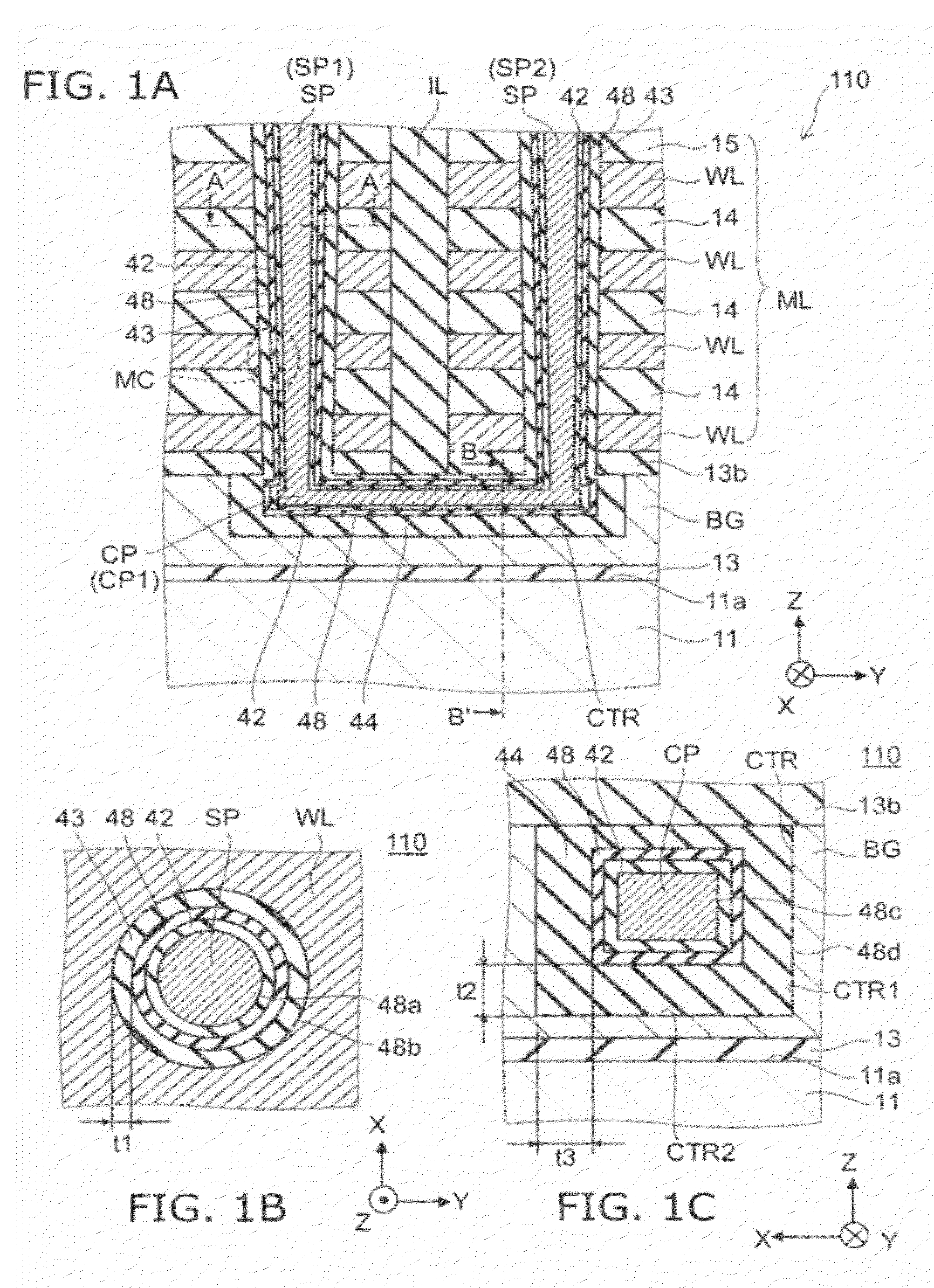
[0025]FIGS. 1A to 1C are schematic cross-sectional views illustrating the configuration of a nonvolatile semiconductor memory device according to a first embodiment.

[0026]Namely, FIG. 1B is a cross-sectional view along line A-A′ of FIG. 1A; and FIG. 1C is a cross-sectional view along line B-B′ of FIG. 1A.

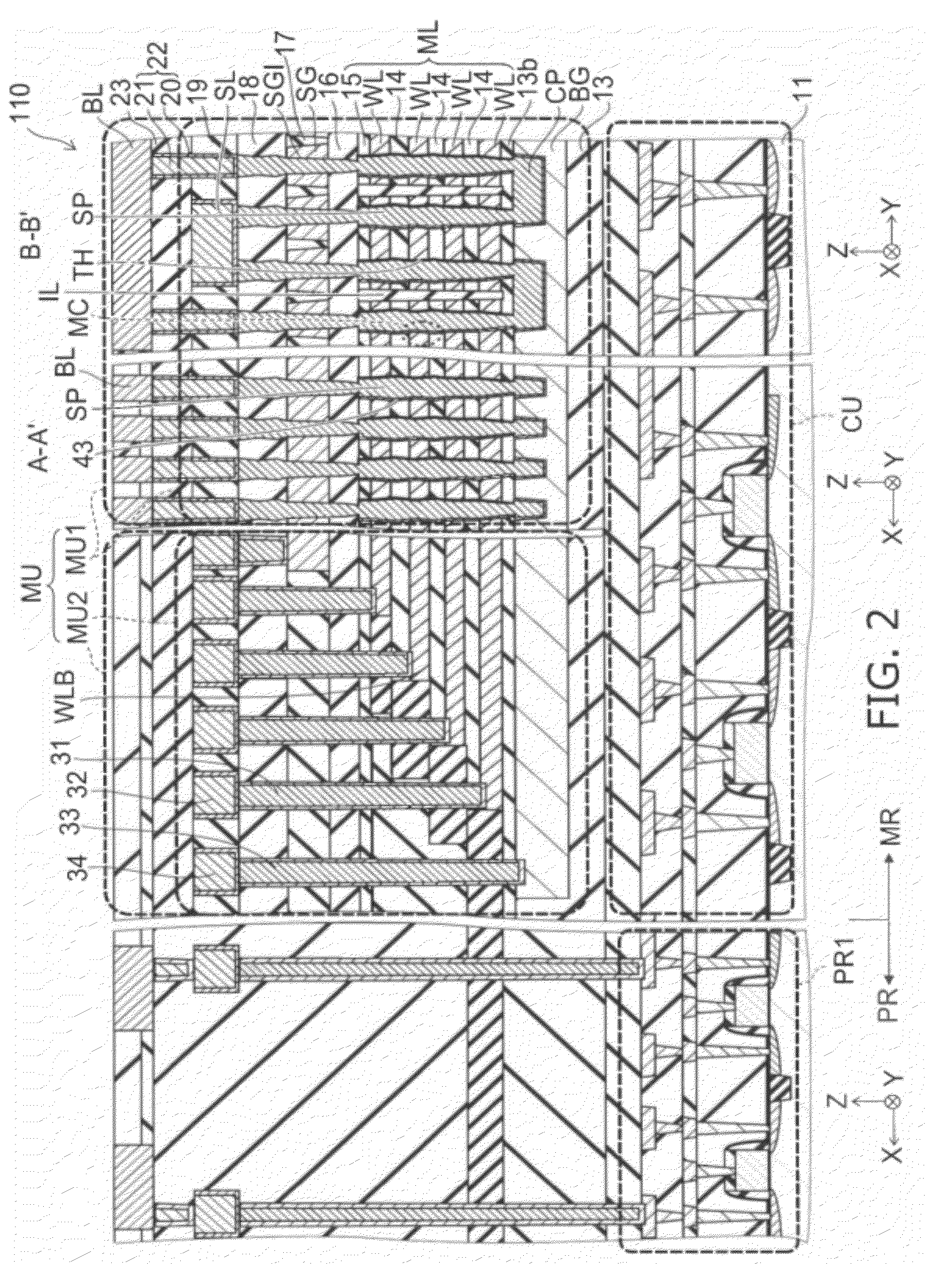
[0027]FIG. 2 is a schematic cross-sectional view illustrating the entire configuration of the nonvolatile semiconductor memory device according to the first embodiment.

[0028]FIG. 3 is a schematic perspective view illustrating the configuration of the nonvolatile semiconductor memory device according to the first embodiment.

[0029]For easier viewing of the drawing in FIG. 3, only the conductive portions are illustrated, and the insulating portions are omitted.

[0030]FIG. 4 is a schematic plan view illustrating the configuration of electrode films of the nonvolatile semiconductor memory device according to the first embodiment.

[0031]FIG. 5 is a schematic cross-sectional view illustratin...

second embodiment

[0164]FIG. 10 is a flowchart illustrating a method for manufacturing a nonvolatile semiconductor memory device according to a second embodiment.

[0165]In the method for manufacturing the nonvolatile semiconductor memory device according to this embodiment, first, the trench CTR is made in a conductive layer (the conductive film BGf forming the back gate BG) provided on the major surface 11a of the semiconductor substrate 11 (the substrate); an insulating film (the insulating film 44a) is formed on the wall face of the trench CTR; and subsequently, the sacrificial layer Sf is filled into the remaining space of the trench CTR as illustrated in FIG. 10 (step S110).

[0166]In other words, the processing described in regard to FIGS. 7A to 7C is implemented.

[0167]Then, the multiple electrode films WL are alternately stacked with the multiple inter-electrode insulating films 14 on the conductive layer (the conductive film BGf), the insulating film (the insulating film 44a), and the sacrificia...


PUM


Abstract

A nonvolatile semiconductor memory device, includes: a stacked structural unit including electrode films alternately stacked with inter-electrode insulating films; first and second semiconductor pillars piercing the stacked structural unit; a connection portion semiconductor layer electrically connect the first and second semiconductor pillars; a connection portion conductive layer provided to oppose the connection portion semiconductor layer; a memory layer and an inner insulating film provided between the first and semiconductor pillars and each of the electrode films, and between the connection portion conductive layer and the connection portion semiconductor layer; an outer insulating film provided between the memory layer and each of the electrode films; and a connection portion outer insulating film provided between the memory layer and the connection portion conductive layer. The connection portion outer insulating film has a film thickness thicker than a film thickness of the outer insulating film.

Description

CROSS-REFERENCE TO RELATED APPLICATIONS[0001]This application is based upon and claims the benefit of priority from the prior Japanese Patent Application No. 2009-169954, filed on Jul. 21, 2009; the entire contents of which are incorporated herein by reference.BACKGROUND[0002]1. Field[0003]Embodiments of the invention relate generally to a nonvolatile semiconductor memory device and a method for manufacturing the same.[0004]2. Background Art[0005]Nonvolatile semiconductor memory devices (memory) conventionally have elements integrated in a two-dimensional plane on a silicon substrate. Although the dimensions of one element are reduced (downscaled) to increase the memory capacity of the memory, such downscaling in recent years has become difficult in regard to both cost and technology.[0006]On the other hand, although many ideas for three-dimensional memory, etc., have been proposed, three-dimensional devices generally require processes including at least three lithography processes ...

Claims


Application Information

Patent Timeline
Patent Type & Authority Patents(United States)
IPC IPC(8): H01L21/00
CPCH01L27/11524H01L27/11526H01L27/11529H01L27/11551H01L27/11556H10B41/40H10B41/41H10B41/20H10B41/35H10B41/27
Inventor FUJIWARA, TOMOKOKATSUMATA, RYOTAKITO, MASARUFUKUZUMI, YOSHIAKIKIDOH, MASARUTANAKA, HIROYASUKOMORI, YOSUKEISHIDUKI, MEGUMIMATSUNAMI, JUNYAAOCHI, HIDEAKIKIRISAWA, RYOUHEIMIKAJIRI, YOSHIMASAOOTA, SHIGETO
Owner KK TOSHIBA
Why Eureka
Try Eureka