Laser diode structure with reduced interference signals

a technology of interference signals and laser diodes, applied in lasers, laser construction details, semiconductor laser optical devices, etc., can solve the problems of optical noise that reduces the signal resolution of high-resolution testing devices, and achieve the effect of improving the resolution of test signals

Active Publication Date: 2012-06-12
AXETRIS AG
View PDF12 Cites 19 Cited by
  • Summary
  • Abstract
  • Description
  • Claims
  • Application Information

AI Technical Summary

Benefits of technology

[0005]The invention addresses the problem of significantly reducing or completely eliminating the etalons and / or the self-mixing of a laser diode due to back-reflections inside the housing of the laser diode structure in order to improve the resolution of the test signal.
[0012]Preferably, a microactuator in the form of a piezo oscillating element, an electro-mechanical drive system, or an electrostatic or a thermal control device is used as actuator. In all possible embodiments of the laser diode structure according to the invention, the power device also comprises a control system for applying a direct voltage and / or an alternating voltage portion to the actuator. In a favorite embodiment, the direct voltage portion of the actuator control system is used to align the laser beam with the radiation detector. Here, the control system is able to vary the amplitude, the frequency, and / or the wave shape of the alternating voltage portion for optimal time-averaging of the back-reflected laser light. For example, for the time-averaging of the back-reflections of laser light by means of a movable collimator lens, a microlens made of silicon may be provided that is attached to the actuator in such a way that the laser aperture is located in the focal plane of the microlens. The collimating microlens is positioned in such a way that it is several hundred micrometers distant, in the direction of extension of the laser beam (z-direction), from the laser aperture of the laser diode, for example the laser aperture of a VCSEL. For the averaging, the actuator is operated with an alternating voltage by the control system of the power device so that the position of the collimator lens above the laser aperture oscillates in the z-direction. The frequency of the alternating voltage is selected high enough to ensure that every measuring point is averaged over a sufficient number of positions. With this process, the etalons and / or self-mixing effects caused by the boundary surface of the microlens are averaged efficiently.
[0013]In a simple embodiment, for example a piezo oscillating element that changes its structural height when an electrical voltage is applied, can be used as actuator. In addition, it is advantageous to arrange the laser aperture in the focal plane of the collimator lens, but not in the focal point of the lens itself. In practice, a lateral displacement of the optical axis of the collimator lens relative to the optical axis of the laser aperture of 30 to 50 μm proved to be optimal. In addition, it is advantageous to attach the actuator lens to the actuator in such a way that the focal plane of the collimator lens is not perpendicular to the beam direction of the laser beam but is inclined at an angle of 10 to 30° relative to the laser beam.
[0015]For the purpose of time-averaging the back-reflections of laser light towards the laser aperture of the laser diode it is also possible to continuously swivel back and forth the axis of the laser beam relative to the axis of the collimator lens. This results in continuously different path lengths for the back-reflections, which has the effect of effectively averaging the related interference effects. In order to continuously swivel the beam axis of the laser beam in an oscillating manner, it is possible, for example, to attach the movable deflecting mirror to the actuator in such a way that the laser beam first hits the mirror surface before reaching the surface of the collimator lens. In order to keep the structural size of the laser diode structure small, it is possible, for example, to use a so-called micromirror with a mirror surface size of only a few square millimeters.
[0016]The deflecting mirror can be rotated around at least one axis. Typically, such a micromirror is operated with a direct voltage on which an alternating voltage is superimposed. By means of the direct voltage, the neutral position of the micromirror can be defined, while the alternating voltage serves to continuously swivel the micromirror back and forth around the neutral position. Since over an optical path length of the laser beam of approximately 1 to 2 mm it is necessary to generate path differences of approximately 1 to 2 μm for the effective time-averaging of the back-reflections, very small deflections of the deflecting mirror around the neutral position are sufficient for this. By rotating the axis of the laser beam, these path differences are continuously being generated for all possible reflecting surfaces so that an arrangement of this type allows efficient averaging across all occurring optical interferences. This largely suppresses interfering effects caused by etalons or self-mixing. The setting of the neutral position of the laser beam by means of the direct voltage portion that moves the micromirror can additionally be employed for the automatic adjustment of the laser beam towards a photo detector. Here, a micromirror that can be deflected around two axes by the actuator is an advantage. It appears that a deflecting mirror of this type is clearly superior to a mirror that can be deflected in a single axis only.

Problems solved by technology

Both effects cause optical noise that reduces the signal resolution in high-resolution testing devices and with weak gas absorptions.

Method used


Image

  • Laser diode structure with reduced interference signals
  • Laser diode structure with reduced interference signals
  • Laser diode structure with reduced interference signals

Examples


first embodiment

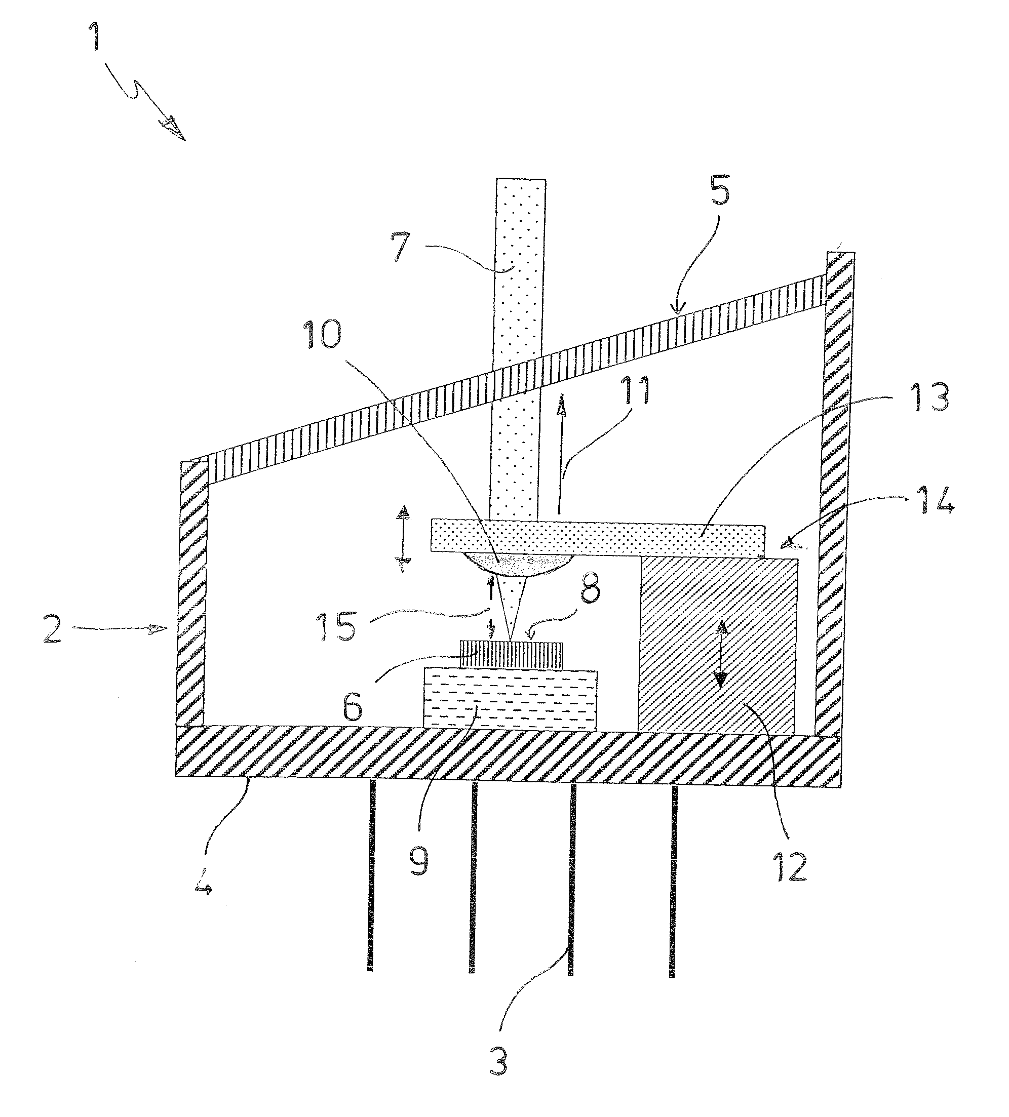
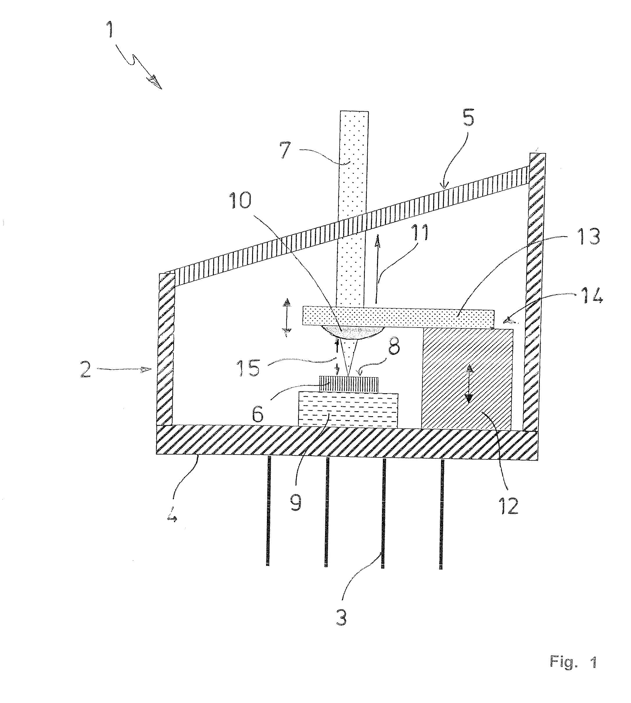
[0023]FIG. 1 shows a laser diode structure 1 according to the invention, with a hermetically enclosed housing 2 that comprises a number of electrical connections 3 on a housing bottom 4 of the housing 2. Opposite the housing bottom 4, an exit window 5 is provided for the exit from the housing 2 of a laser beam 7 emitted by a laser diode 6. The exit window 5 extends at an angle to the housing bottom 4 of the housing 2 and to a laser aperture 8 of the laser diode 6. The laser diode 6 is mounted on a temperature control device 9 that is formed by a Peltier element. The Peltier element 9 is arranged on the housing bottom 4 and carries the laser diode 6 on a cold flat surface. With its warm flat surface on the opposite side, the Peltier element 9 is connected with the housing bottom 4 in a thermally well-conductive way. In addition, beside the laser diode 6, a thermistor (not shown) that serves as thermal sensor and controls the operating current of the Peltier element may be arranged on...

third embodiment

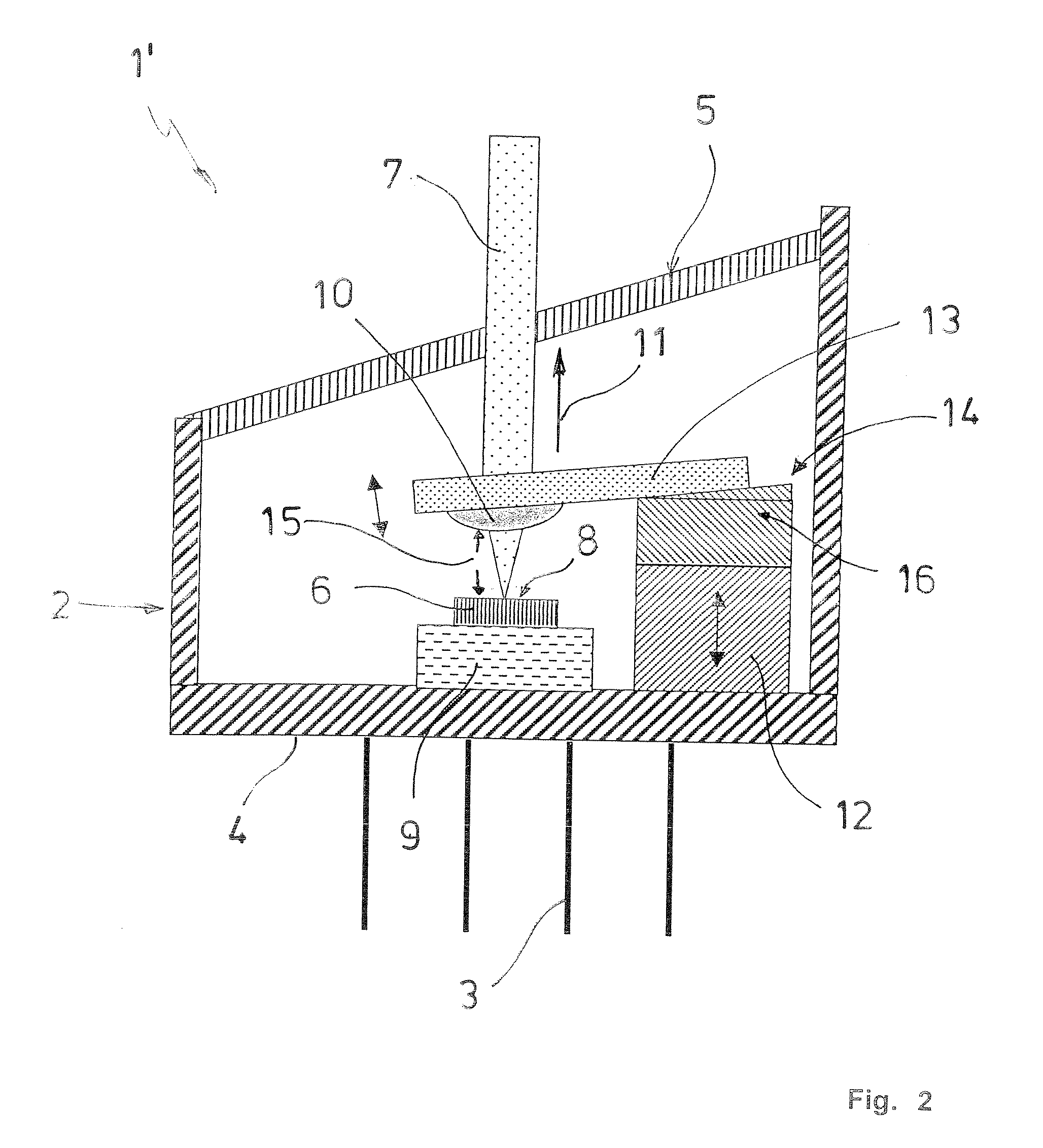
[0029]FIG. 3 shows the laser diode structure according to the invention. In the laser diode structure 1″ shown here, the collimator lens 10 simultaneously forms the exit window 5 which in this case is arranged parallel to the housing bottom 4 of the housing 2. Like the laser diodes 6 in the laser diode structures 1, 1′, the laser diode 6′ is carried by a temperature control device 9 that is arranged eccentrically on the housing bottom 4. Compared with the laser diodes 6 used in the laser diode structures 1, 1′, the laser diode 6′ has a laser aperture 8 that is provided laterally on the laser diode 6′. After exiting from the laser aperture 8, the laser beam 7 is deflected by a deflecting mirror 17 in the form of a micromirror in the direction of the collimator lens 10.

[0030]On the one hand, the micromirror 17 is swivelably connected to a holder 18 that is attached to the housing bottom 4 next to the temperature control device 9, and, on the other hand, it is connected, at a distance ...


PUM


Abstract

A laser diode structure for generating a collimated or divergent laser beam, preferably for application in gas detection, with a laser diode arranged in a closed housing, with the housing comprising a housing bottom, an exit window, electrical connections, a temperature control device for the laser diode, and an optical element for influencing the laser beam. The temperature control device carrying the laser diode is arranged on the housing bottom and the optical element is positioned at a distance from the laser diode. The invention proposes an electrically controllable power device for the cyclic alteration of the position and / or alignment of the optical element in relation to the laser diode so that the optical path length for the laser beam in the housing changes periodically. The oscillating motion of the optical element has the effect of time-averaging the etalon and / or self-mixing effects caused by the back-reflections of the laser beam in the housing, thereby reducing the optical noise of the laser diode structure.

Description

CROSS-REFERENCE TO RELATED APPLICATION[0001]The present application claims priority under 35 USC §119 to European Patent Application No. 10 002 153.4 filed Mar. 3, 2010, the entire disclosure of which is incorporated herein by reference.TECHNICAL FIELD OF THE INVENTION[0002]The invention concerns a laser diode structure for generating a laser beam, preferably for application in gas detection. The laser diode structure has a laser diode arranged in a closed housing wherein the housing comprises a housing bottom, an exit window for the laser beam, electrical connections, a temperature control device for the laser diode, and an optical element for guiding and / or shaping the laser beam, with the optical element positioned at a distance from the laser diode. The temperature control device is arranged on the housing bottom and carries the laser diode.[0003]Such a laser diode structure can be used, for example as a narrow-band radiation source in conjunction with a corresponding radiation ...

Claims


Application Information

Patent Timeline
Patent Type & Authority Patents(United States)
IPC IPC(8): H01S3/04
CPCH01S5/02288G01N2021/399H01S5/005H01S5/0071H01S5/0085H01S5/02292H01S5/02296H01S5/02415H01S5/0656H01S2301/02H01S5/02255H01S5/02257H01S5/02253
Inventor GAILLARD, MATHIEUWILLING, BERTMANZENEDER, STEFAN
Owner AXETRIS AG
Why Eureka
Try Eureka