
Light output device

a technology of light output device and led glass, which is applied in the direction of lighting and heating apparatus, process and machine control, instruments, etc., can solve the problems of high electrical losses in these wires, add to the cost of the device, and difficulty in providing a structure which allows individual leds in the glass

Active Publication Date: 2012-07-24
SIGNIFY HLDG BV
View PDF13 Cites 30 Cited by
  • Summary
  • Abstract
  • Description
  • Claims
  • Application Information

AI Technical Summary

Benefits of technology

The invention is a light output device that includes a substrate arrangement with multiple light source devices integrated into it. The light source devices are arranged in anti-parallel, which means they are arranged in a way that their electrical contacts are opposite each other. This arrangement allows for independent control of each light source device, reducing resistive losses and improving control accuracy. The device also includes a power source that provides independent control of the light source devices. The light source devices can be LED devices, and the substrate arrangement can be made using a transparent conductor arrangement or a semi-transparent conductor arrangement. The invention also provides a method for driving the light output device and a lighting system comprising the light output device and a lighting controller. The technical effects of the invention include improved control accuracy, reduced resistive losses, and improved performance of the light output device.

Problems solved by technology

One problem with this type of device is that it is difficult to provide a structure which enables individual LEDs in the glass to be turned on and off, for example in order to display an image, or a dynamic pattern.
This is difficult, because a two-dimensional pattern of transparent electrodes is desired, but crossovers need to be avoided if the layer structure is to be kept simple.
If individual wires are used for each LED (instead of a two dimensional pattern), this results in very high wire resistances (for example ITO electrodes), leading to high electrical losses in these wires.
An alternative is to place several sheets of LEDs in glass behind each other, which adds to the cost of the device.
Another problem is how to dynamically control the color of the LEDs in glass.
Currently, this can again only be achieved by adding extra wires, leading again to thinner ITO wires and thus to extra electronic losses.
Furthermore, LED devices are not typically suitable for ac drive voltages, as they have diode electrical characteristics.

Method used


Image

  • Light output device
  • Light output device
  • Light output device

Examples


Embodiment Construction

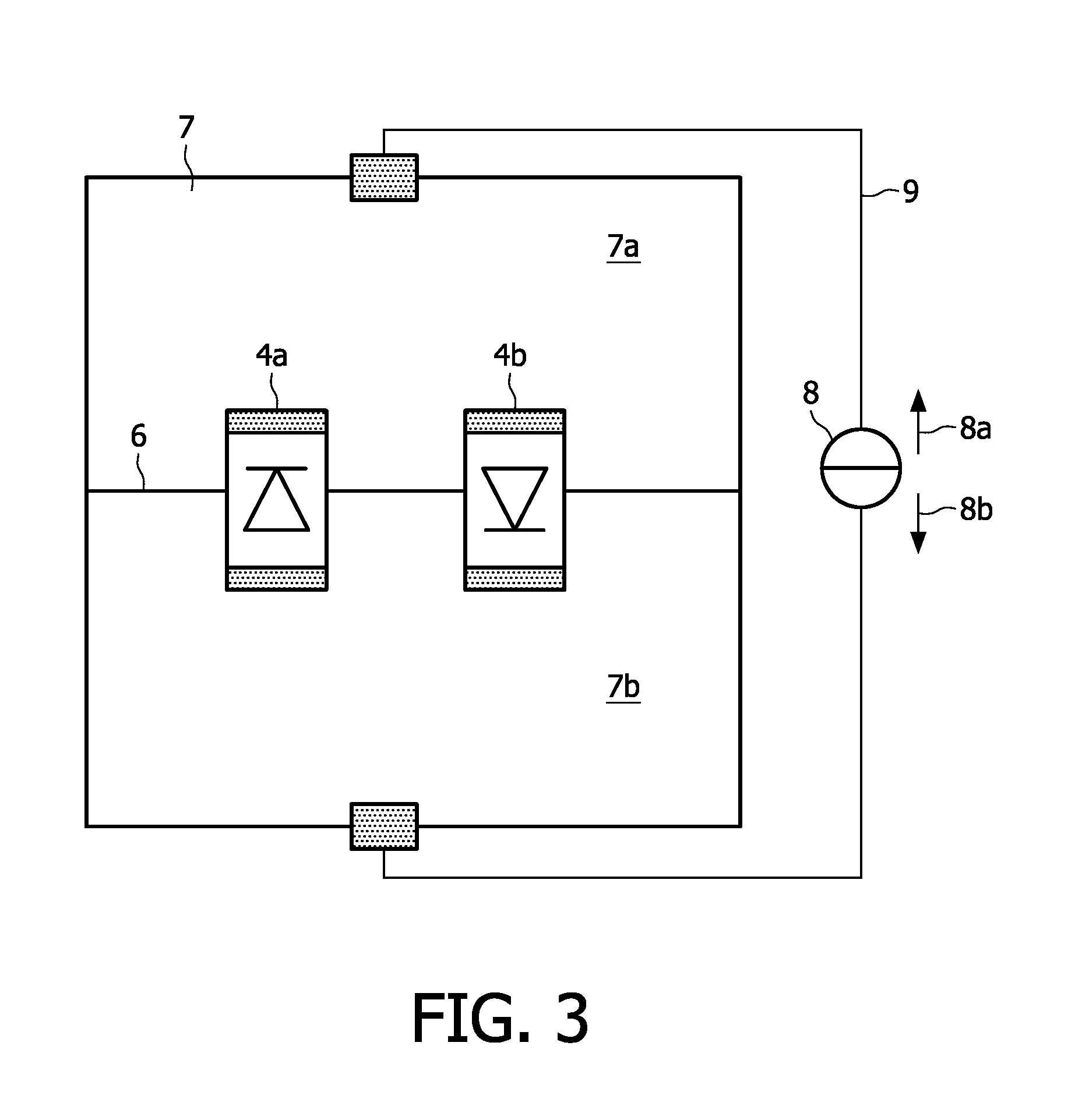
[0040]The structure of an LED in glass illumination device is shown in FIG. 2. The lighting device comprises glass plates 1 and 2. Between the glass plates are (semi-) transparent electrodes 7a and 7b (for example formed using ITO), and a LED 4 connected to the transparent electrodes 7a and 7b. A layer of thermoplastic material 5 is provided between glass plates 1 and 2 (for example PVB or UV resin).

[0041]The glass plates typically may have a thickness of 1.1 mm-2.1 mm. The spacing between the electrodes connecting to the LED is typically 0.01-3 mm, for example around 0.15 mm. The thermoplastic layer has a typical thickness of 0.3 mm-2 mm, and the electrical resistance of the electrodes is in the range 2-80 Ohm, or 10-30 Ohms / square.

[0042]The electrodes are preferably substantially transparent, so that they are imperceptible to a viewer in normal use of the device. If the conductor arrangement does not introduce a variation in light transmission (for example because it is not patter...


PUM

PropertyMeasurementUnit
electrical resistanceaaaaaaaaaa
transparencyaaaaaaaaaa

Abstract

A light output device comprises a substrate arrangement with a plurality of light source device arrangements integrated into the structure of the substrate arrangement. The plurality of light source device arrangements comprise at least first and second light source devices (4a,4b) which are arranged in anti-parallel. This arrangement mounts at least two light source devices in anti-parallel within an integrated light source structure, so that they can be controlled independently from shared control lines.

Description

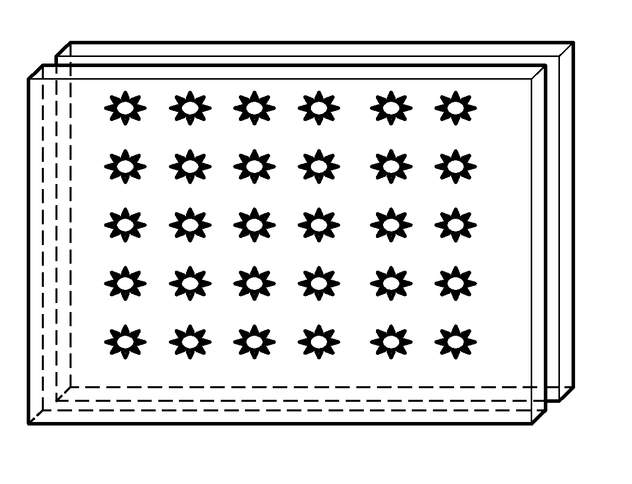
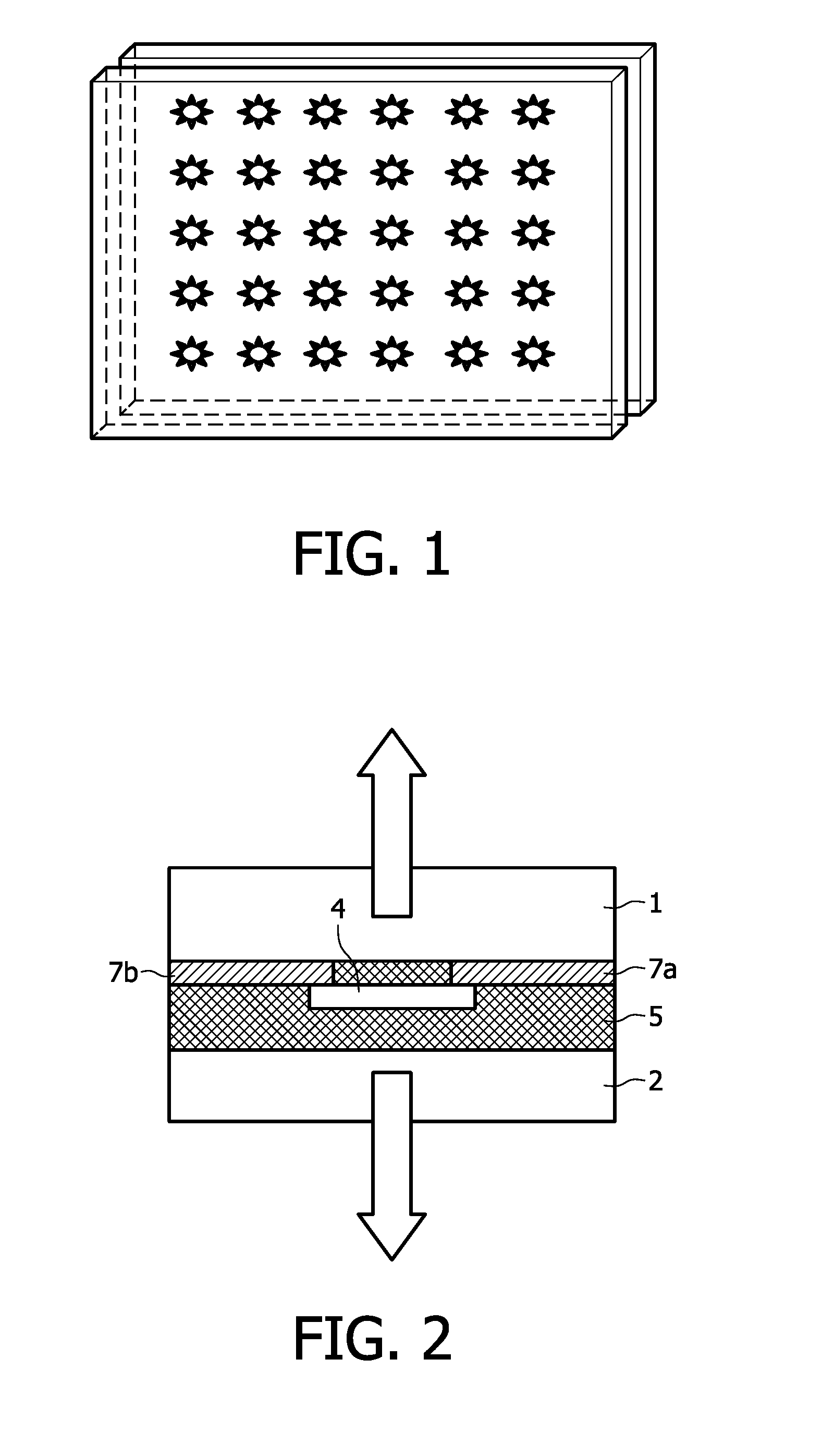
FIELD OF THE INVENTION[0001]This invention relates to light output devices, in particular using discrete light sources associated with a light transmissive substrate structure.BACKGROUND OF THE INVENTION[0002]One known example of this type of lighting device is a so-called “LED in glass” device. An example is shown in FIG. 1. Typically a glass plate is used, with a transparent conductive coating (for example ITO) forming electrodes. The conductive coating is patterned in order to make the electrodes, that are connected to a semiconductor LED device. The assembly is completed by laminating the glass, with the LEDs inside a thermoplastic layer (for example polyvinyl butyral, PVB). The glass used may be safety glass. Applications of this type of device are shelves, showcases, facades, office partitions, wall cladding, and decorative lighting. The lighting device can be used for illumination of other objects, for display of an image, or simply for decorative purposes.[0003]One problem w...

Claims


Application Information

Patent Timeline
Patent Type & Authority Patents(United States)
IPC IPC(8): H05B41/24F21K99/00H05B44/00
CPCB32B17/10036B32B17/10174F21V33/006B32B17/10761Y10S362/80F21Y2101/02B32B17/10541F21Y2115/10
Inventor VAN HERPEN, MAARTEN MARINUS JOHANNES WILHELMUSVERMEULEN, MARKUS CORNELIUSVANLIER, GERARDUS JOHANNES JOSEPHUS
Owner SIGNIFY HLDG BV
Learn More