

Interconnect structure having a via with a via gouging feature and dielectric liner sidewalls for BEOL integration
a technology of dielectric liner sidewalls and interconnect structures, which is applied in the field of semiconductor interconnect structures, can solve the problems of reducing the quality of diffusion barriers, and increasing the difficulty of wiring, so as to improve the reliability of wiring
- Summary
- Abstract
- Description
- Claims
- Application Information
AI Technical Summary
Benefits of technology
Problems solved by technology
Method used
Image

Examples
Embodiment Construction
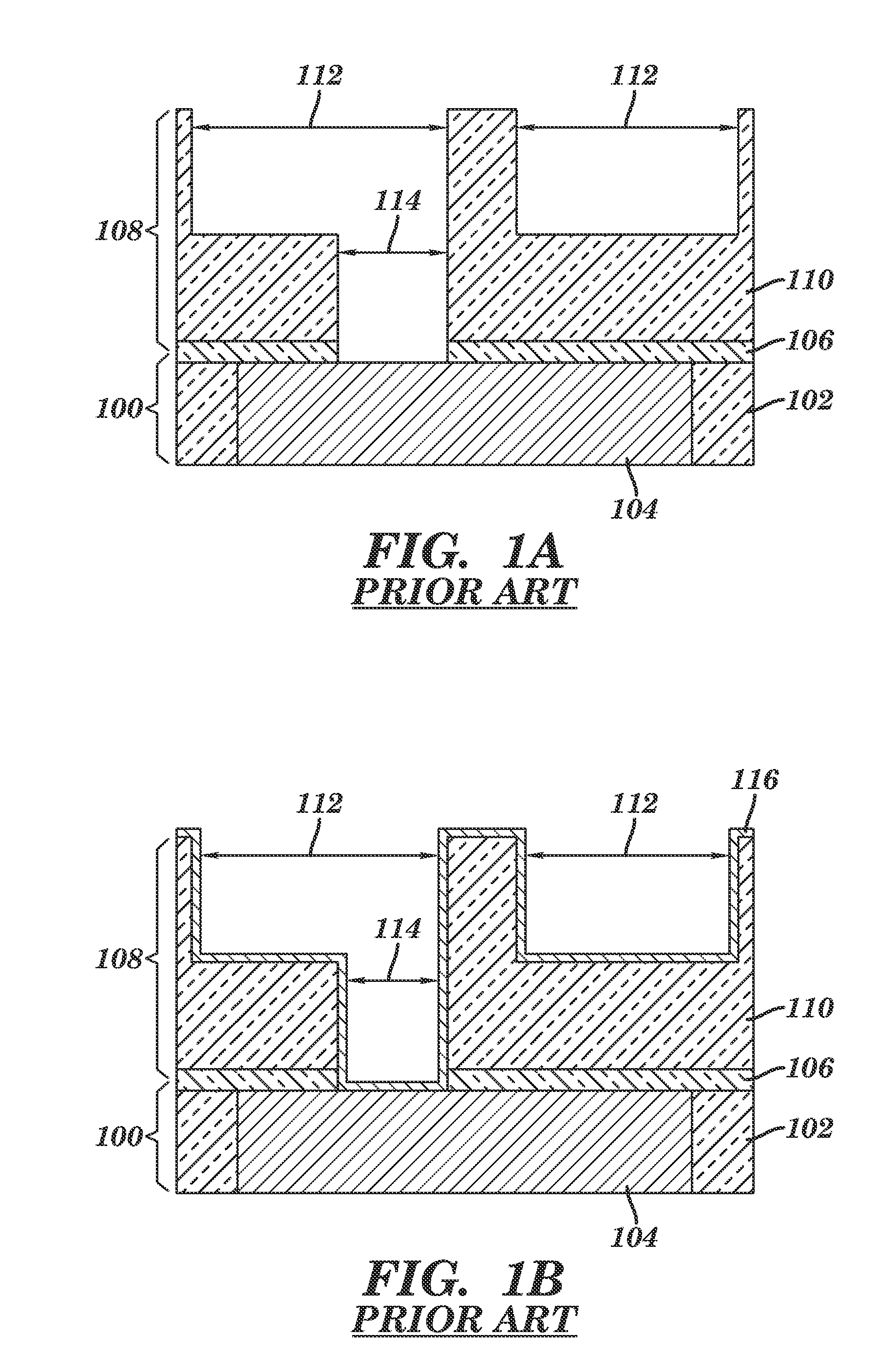
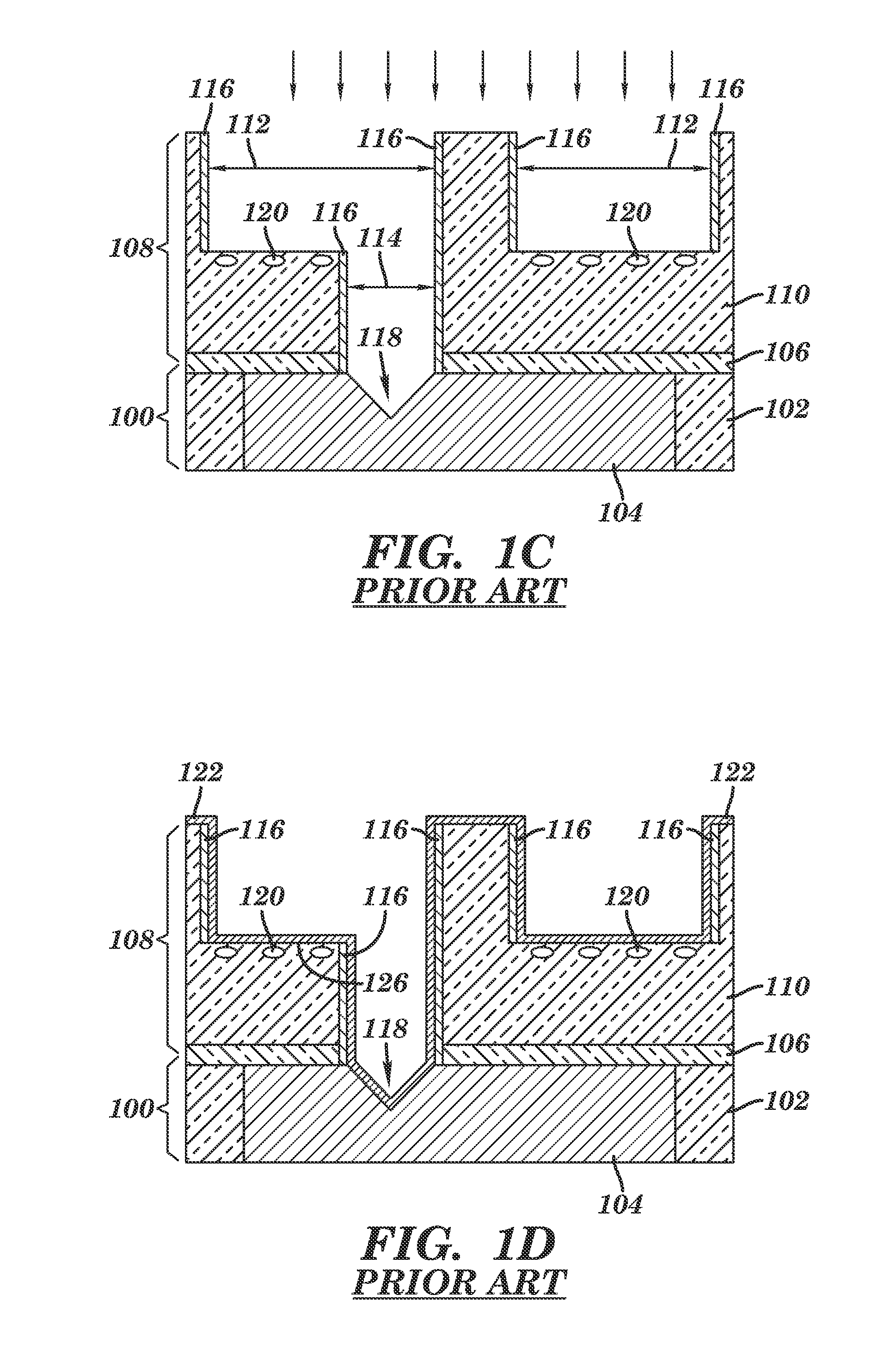
[0016]The present invention will now be described more fully hereinafter with reference to the accompanying drawings in which preferred embodiments of the invention are shown. This invention may, however, be embodied in many different forms and should not be construed as limited to the illustrated embodiments set forth herein. Rather, these embodiments are provided so that this disclosure will be thorough and complete, and will fully convey the scope of the invention to those skilled in the art. Like numerals refer to like features throughout.
[0017]It will be understood that when an element, such as a layer, is referred to as being “on” or “over” another element, it can be directly on the other element or intervening elements may also be present. In contrast, when an element is referred to as being “directly on” or “directly over” another element, there are no intervening elements present.
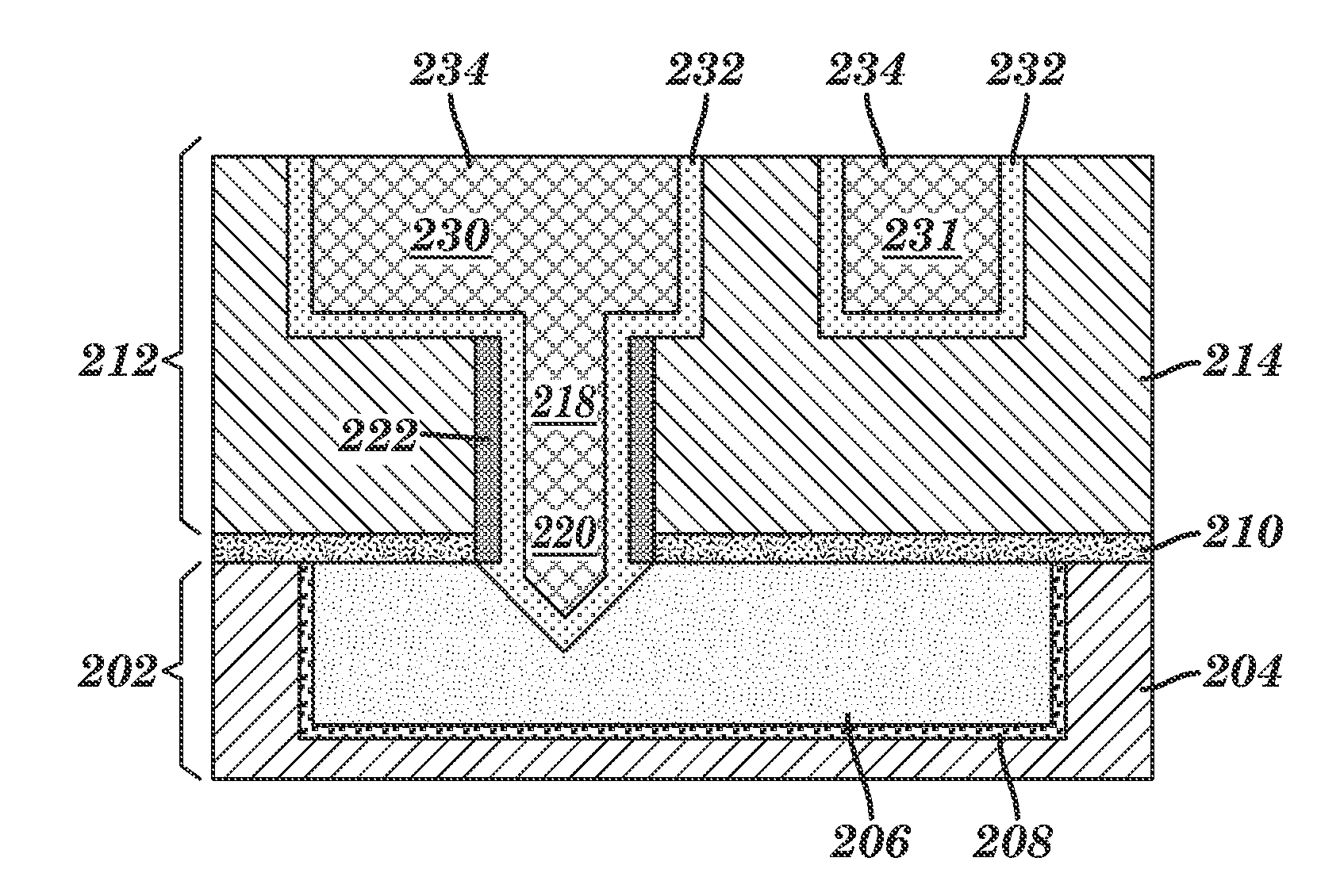
[0018]The present invention provides an interconnect structure in which at least one via has a ...
PUM
| Property | Measurement | Unit |
|---|---|---|
| thickness | aaaaa | aaaaa |
| thickness | aaaaa | aaaaa |
| dielectric constant | aaaaa | aaaaa |
Abstract
Description
Claims
Application Information