

Method for the formation of copper wiring films
a technology of wiring film and copper, applied in the direction of superimposed coating process, semiconductor/solid-state device details, coatings, etc., can solve the problems of substrate damage, brought to the adhesion-improving effect, etc., and achieve the effect of improving adhesion
- Summary
- Abstract
- Description
- Claims
- Application Information
AI Technical Summary
Benefits of technology
Problems solved by technology
Method used
Image

Examples
embodiment
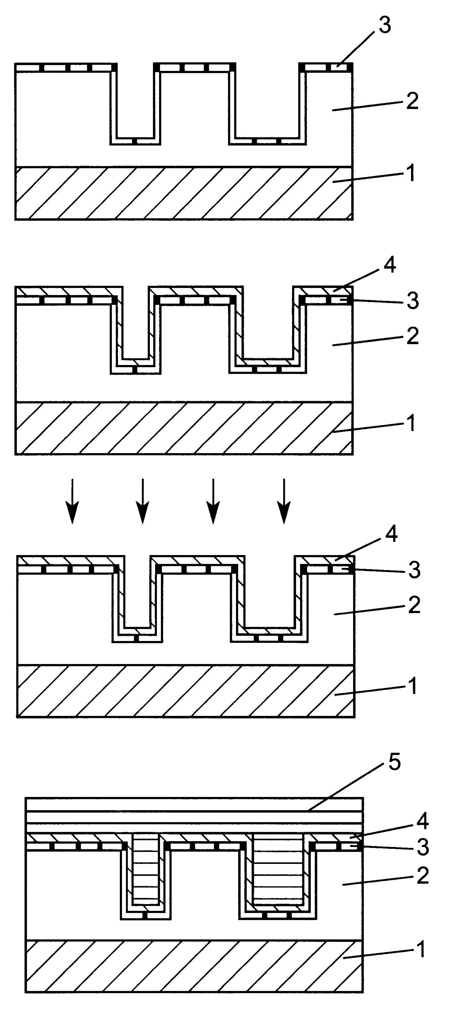
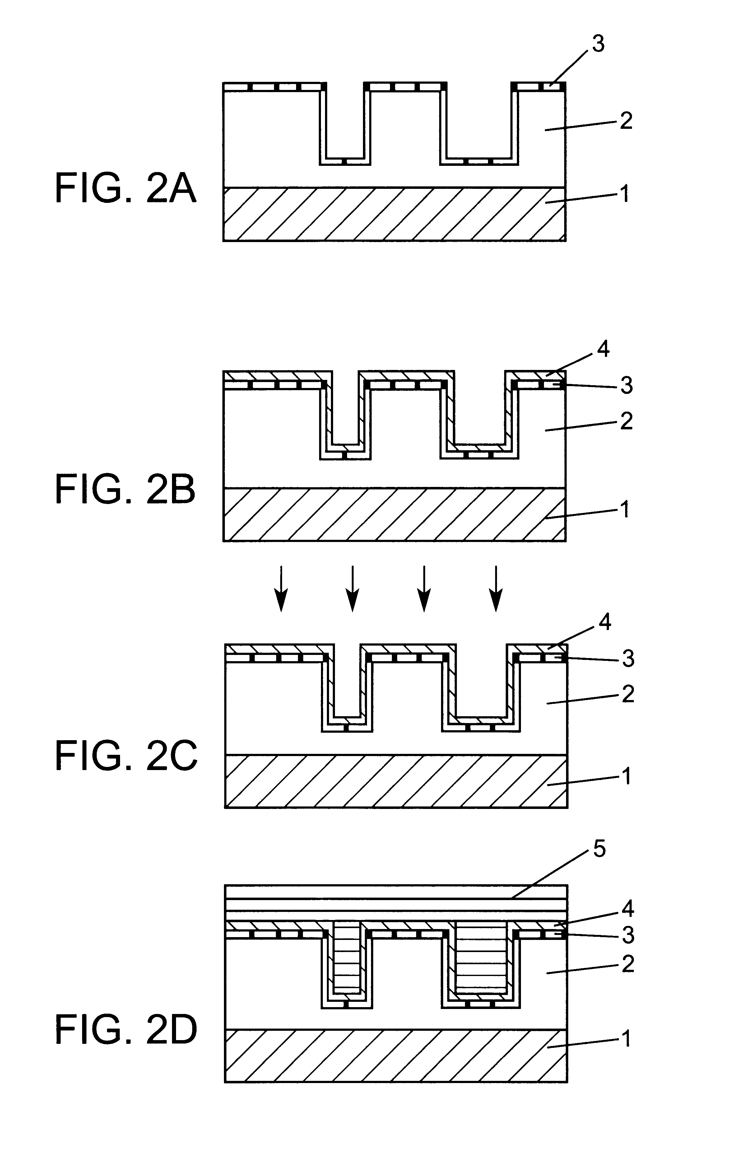
A Cu seed film (the first copper film indicated by the number 4 in FIG. 2) was formed with a film thickness of 30 nm as a structure approaching that of an actual semiconductor device using the copper wiring film forming method of the invention, and verification of the increased adhesion with a sample where this film was used as the electrode for copper electroplating was carried out.
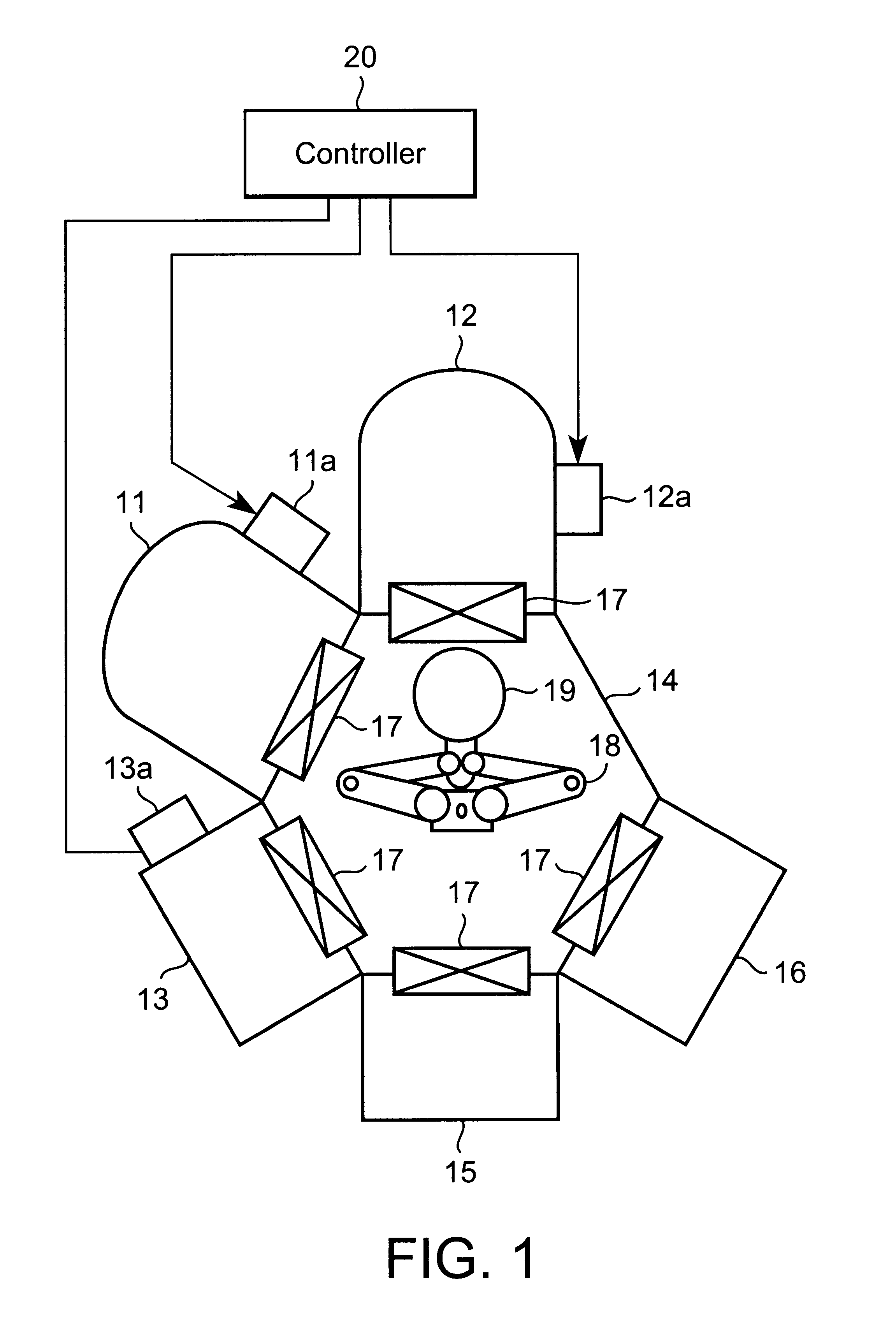
The sample for adhesion evaluation purposes was obtained using the apparatus shown in FIG. 1 (described earlier) with treatment under consistent vacuum conditions in the TiN for diffusion barrier purposes CVD chamber 11 and the copper film CVD chamber 12, and then using an electric furnace for the annealing process.
The annealing conditions in the electric furnace were 13 KPa under an Ar gas atmosphere with an annealing temperature of 400.degree. C. and an annealing time of 30 minutes.
Subsequently, a second copper film (number 5 in FIG. 2) was formed by copper electroplating using the Cu seed film (first ...
PUM
| Property | Measurement | Unit |
|---|---|---|
| temperature | aaaaa | aaaaa |
| thickness | aaaaa | aaaaa |
| temperature | aaaaa | aaaaa |
Abstract
Description
Claims
Application Information