Tunnel junction structure, forming method thereof and tunnel junction device

A tunnel junction and device technology, applied in semiconductor devices, electrical components, sustainable manufacturing/processing, etc.

Pending Publication Date: 2021-03-19
SUZHOU EVERBRIGHT PHOTONICS +1
View PDF4 Cites 3 Cited by
  • Summary
  • Abstract
  • Description
  • Claims
  • Application Information

AI Technical Summary

Problems solved by technology

[0004] The technical problem to be solved by the present invention is to overcome the problem of how to improve the tunneling peak current of the tunnel junction structure in the prior art

Method used


Image

  • Tunnel junction structure, forming method thereof and tunnel junction device
  • Tunnel junction structure, forming method thereof and tunnel junction device
  • Tunnel junction structure, forming method thereof and tunnel junction device

Examples


Embodiment Construction

[0025] As mentioned in the background, the tunnel junction structure in the prior art has a relatively low tunneling peak current.

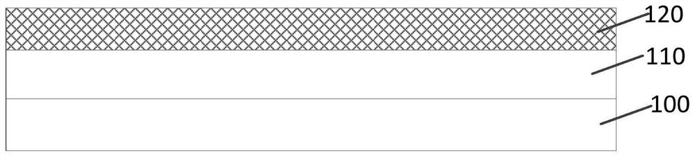
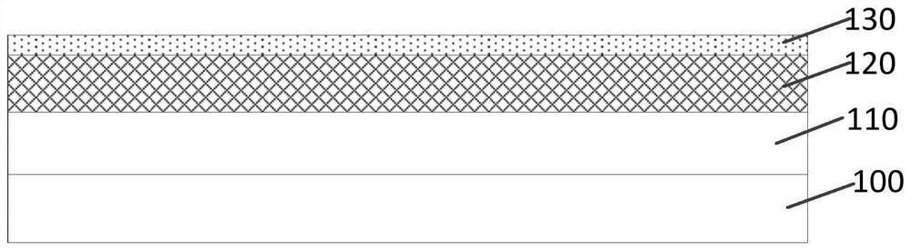
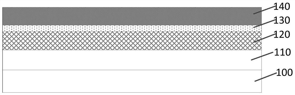
[0026] A tunnel junction structure, comprising: a P-type AlGaAs layer and an N-type InGaP layer in contact with the P-type AlGaAs layer, the P-type AlGaAs layer is doped with C ions, and the N-type InGaP layer is doped with Te ions.

[0027] After research, it was found that according to the following formula:

[0028]

[0029] Neff=(Np*Nn) / (Np+Nn) (2)

[0030] Among them, Neff is the effective doping concentration of the tunnel junction structure, Eg is the bandgap width of the depletion layer, J peak is the tunneling peak current of the tunnel junction structure. Np is the doping concentration of P-type conductive ions in the P-type AlGaAs layer, and Nn is the doping concentration of N-type conductive ions in the N-type InGaP layer.

[0031] The main factor that limits the tunneling peak current of the tunnel junction structure is the qua...


PUM

PropertyMeasurementUnit
Thicknessaaaaaaaaaa

Abstract

The invention discloses a tunnel junction structure, a forming method thereof and a tunnel junction device. The structure comprises a first semiconductor layer, wherein Te ions are arranged in the first semiconductor layer; a second semiconductor layer, wherein the conductive type of the second semiconductor layer is opposite to that of the first semiconductor layer; and a non-doped quantum well layer located between the first semiconductor layer and the second semiconductor layer, wherein the non-doped quantum well layer is suitable for blocking Te diffusion. The tunneling peak current of thetunnel junction structure of the tunnel junction structure is improved.

Description

technical field [0001] The invention relates to the field of semiconductors, in particular to a tunnel junction structure, a forming method thereof, and a tunnel junction device. Background technique [0002] Tunnel junction is the core component of multi-junction solar cell devices to work normally. A high-quality tunnel junction not only needs to meet the requirements of band gap, tunneling peak current, and resistivity, but also needs to overcome the problem of thermal diffusion of dopants in the highly doped layer during material growth. Usually p++AlGaAs / n++InGaP is used as the wide bandgap tunnel junction, InGaP uses highly doped Te, and AlGaAs uses highly doped C. However, Te is used as a surfactant in InGaP, and the doping concentration of Te in InGaP is difficult to reach 2E19atom / cm 3 above. [0003] At present, the tunnel junction formed by the p++AlGaAs / n++InGaP above has a relatively low tunneling peak current. Contents of the invention [0004] The techni...

Claims


Application Information

Patent Timeline
IPC IPC(8): H01L31/0352H01L31/0304H01L31/0725H01L31/0735H01L31/18
CPCH01L31/035236H01L31/03048H01L31/0735H01L31/1844H01L31/0725Y02E10/544Y02P70/50
Inventor 王俊苟于单程洋肖啸郭银涛杨火木
Owner SUZHOU EVERBRIGHT PHOTONICS
Why Eureka
Try Eureka