Back surface structure of IGBT device, preparation method of back surface structure, and IGBT device

A backside structure and device technology, which is applied in semiconductor/solid-state device manufacturing, semiconductor devices, electrical components, etc., can solve the problems of current concentration and turn-off failure at the main junction at the edge of the active region, and achieve excellent breakdown characteristics and small Effects of leakage current and high breakdown voltage

Pending Publication Date: 2020-09-18
GLOBAL ENERGY INTERCONNECTION RES INST CO LTD +2
View PDF4 Cites 1 Cited by
  • Summary
  • Abstract
  • Description
  • Claims
  • Application Information

AI Technical Summary

Problems solved by technology

[0005] Therefore, the technical problem to be solved by the present invention is to overcome the defect that current concentration occurs at the main junction at the edge of the active regi...

Method used


Image

  • Back surface structure of IGBT device, preparation method of back surface structure, and IGBT device
  • Back surface structure of IGBT device, preparation method of back surface structure, and IGBT device
  • Back surface structure of IGBT device, preparation method of back surface structure, and IGBT device

Examples


Embodiment 1

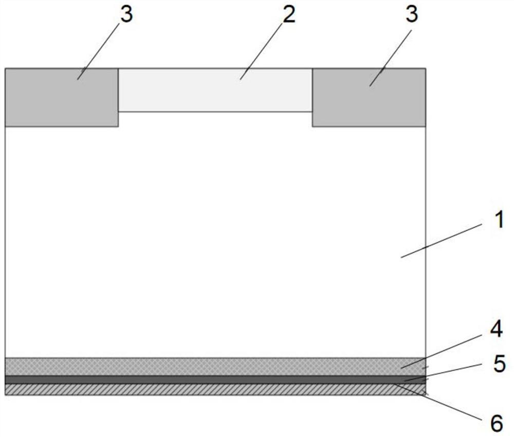
[0036] Such as figure 1 As shown, the present embodiment provides a backside structure of an IGBT device, including a buffer layer 4, and the buffer layer 4 includes a first activation efficiency buffer 41 corresponding to the active region 2 of the IGBT device and a first activation efficiency buffer region 41 corresponding to the terminal region 3 of the IGBT device. The second activation efficiency buffer 42, wherein the activation rate of the first activation efficiency buffer 41 is smaller than the activation efficiency of the second activation efficiency buffer 42.

[0037] Due to the effective doping concentration (N DSPT ) and the current gain of the parasitic transistor PNP of the IGBT device (β PNP ) is inversely proportional to the hole injection efficiency of the terminal region 3 of the IGBT device as the current gain (β PNP ) increases, that is, as the effective doping concentration (N DSPT ) increases, the hole injection efficiency gradually decreases. By se...

Embodiment 2

[0042] This embodiment provides a method for preparing the back structure of an IGBT device, and the IGBT device provided in Embodiment 1 can be obtained, which specifically includes the following steps:

[0043] (1) After completing the preparation of the front structure of the IGBT device, the first ion implantation is carried out to the back side of the wafer to form a buffer layer;

[0044] (2) Carry out the first laser annealing to the buffer layer, wherein, the region corresponding to the active region of the IGBT device in the buffer layer forms the first activation efficiency buffer zone, and the region corresponding to the terminal region of the IGBT device in the buffer layer forms the second Activate efficiency buffer. Specifically, the dose of the first ion implantation is 5E13cm -2 -1E14cm -2 , the implanted element is phosphorus; the formation condition of the first activation efficiency buffer zone is that the laser wavelength is 510-550nm, and the laser energ...


PUM


Abstract

The invention provides a back surface structure of an IGBT device, a preparation method of the back surface structure and the IGBT device. An area, corresponding to an active area of the IGBT device,in a buffer layer is set as a first activation efficiency buffer area; an area corresponding to a terminal area of the IGBT device is set as a second activation efficiency buffer area, and the activation rate of the second activation efficiency buffer area is greater than the activation efficiency of the first activation efficiency buffer area, so that the hole injection efficiency of the terminalarea is reduced; when the IGBT device chip is turned off due to overcurrent, holes injected into the terminal area are collected through a main junction when the IGBT is turned off, so that the phenomenon of current concentration at the main junction at the edge of the active area is reduced, and the overcurrent turn-off performance of the device is improved.

Description

technical field [0001] The invention relates to the technical field of semiconductor devices, in particular to a back structure of an IGBT device, a preparation method thereof, and an IGBT device. Background technique [0002] IGBT (Insulated Gate Bipolar Transistor), also known as insulated gate bipolar transistor, is currently the most representative power electronic device. IGBT is a composite full-control-voltage-driven-power semiconductor device composed of BJT (bipolar junction transistor) and MOS (insulated gate field effect transistor). It has the characteristics of self-shutoff, so it has both BJT devices and The advantages of MOS devices, such as voltage-controlled switching, high operating frequency, simple drive control circuit, and bipolar conduction, etc. Since the birth of IGBT technology, after more than 30 years of development, IGBT technology has undergone four generations of changes, followed by the first generation planar gate punch-through type, the sec...

Claims


Application Information

Patent Timeline
IPC IPC(8): H01L29/06H01L29/739H01L21/331
CPCH01L29/0623H01L29/0638H01L29/0684H01L29/7395H01L29/66333H01L21/268H01L21/26513H01L29/0834
Inventor 李立金锐王耀华董少华刘江高明超吴军民
Owner GLOBAL ENERGY INTERCONNECTION RES INST CO LTD
Why Eureka
Try Eureka