SiC MOSFET structure and manufacturing method thereof

A manufacturing method and epitaxial layer technology, applied in semiconductor/solid-state device manufacturing, semiconductor devices, electrical components, etc., can solve problems such as device performance degradation, ohmic contact increase, and reliability reduction, so as to reduce ohmic contact resistance and reduce Effect of specific contact resistance and reduction of device loss

Pending Publication Date: 2022-04-12
安徽长飞先进半导体有限公司
View PDF0 Cites 1 Cited by
  • Summary
  • Abstract
  • Description
  • Claims
  • Application Information

AI Technical Summary

Problems solved by technology

[0003] Unlike traditional Si materials, since doped impurity ions hardly diffuse in SiC materials even at high temperatures of 1700°C, self-aligned channels cannot be formed in the form of double diffusion as in Si materials
In the manufacture of SiC MOSFETs, it is generally necessary to form a channel through well implantation and source implantation twice, but this method is very dependent on the registration accuracy of lithography. For the manufacture of MOSFET devices with channel lengths below 0.6 μm, The deviation introduced by this manufacturing method is likely to cause a large difference in the length of the channels on both sides, which in turn will cause the performance of the device to deteriorate and the reliability to decrease.
In order to reduce the dependence on the overlay accuracy of the lithography machine in the manufacture of SiC MOSFETs, there are currently three processes used to form the self-aligned trenches of SiC MOSFETs, namely the sidewall self-alignment process and the polysilicon oxidation self-alignment process. and inclined mask implantation self-alignment process, although the self-alignment process can solve the problem of unequal channel lengths on both sides of the device, but because the source implantation is generally heavily doped, and in order to suppress the conduction of the parasitic diode in the MOSFET, it is necessary The same impurity is implanted in the source region as the well region, and the implantation is generally heavily doped, so that a very high compensation doping is introduced into the source contact implantation region, resulting in low impurity activation efficiency and increased ohmic contact.

Method used


Image

  • SiC MOSFET structure and manufacturing method thereof
  • SiC MOSFET structure and manufacturing method thereof
  • SiC MOSFET structure and manufacturing method thereof

Examples


Embodiment 1

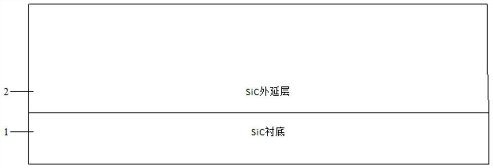
[0077] Such as figure 2 As shown, the RCA method is used to clean the silicon carbide epitaxial wafer, and BOE (buffered oxide etch) or DHF (diluted HF) is used to remove the natural oxide on the silicon carbide surface to obtain a clean silicon carbide epitaxial wafer.

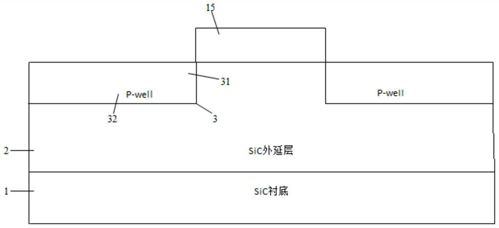
[0078] Such as image 3 As shown, on the clean SiC surface, a mask is deposited by means of deposition. This mask is the P-well implant mask 15. The type of mask can be polysilicon formed by LPCVD deposition, silicon dioxide or PECVD deposition. deposited silicon dioxide, USG, etc., and use photoresist to coat the P-well implantation mask on the P-well implantation mask to protect the P-well implantation mask, and expose the P-well implantation mask 15 corresponding to the P-well implantation area development, and through photolithography and dry etching, the P-well mask pattern is transferred to the mask layer, and Al ion implantation is performed to form a P-well region.

[0079] Such as Pic 4-1 As sho...

Embodiment 2

[0093] Such as figure 2 As shown, the RCA method is used to clean the silicon carbide epitaxial wafer, and BOE (buffered oxide etch) or DHF (diluted HF) is used to remove the natural oxide on the silicon carbide surface to obtain a clean silicon carbide epitaxial wafer.

[0094] Such as image 3 As shown, on the clean SiC surface, a mask is deposited by means of deposition. This mask is the P-well implant mask 15. The type of the mask is polysilicon formed by LPCVD deposition, and it is coated with photoresist. The P-well implantation mask is protected on the P-well implantation mask, and the P-well implantation mask 15 corresponding to the P-well implantation area is exposed and developed, and the P-well implantation is formed by photolithography and dry etching. The mask pattern is transferred to the mask layer, and Al ions are implanted to form a P-well region.

[0095] Such as Figure 4-2 As shown, without removing the P-well mask pattern, put the wafer with the polysi...


PUM

PropertyMeasurementUnit
thicknessaaaaaaaaaa

Abstract

The invention discloses a SiC MOSFET structure which comprises a SiC substrate layer, a SiC epitaxial layer, a P-well region, a P + region and an N + region, the SiC epitaxial layer grows on the SiC substrate layer and covers the SiC substrate layer, and the P-well region, the P + region and the N + region are arranged on the side, away from the SiC substrate layer, of the SiC epitaxial layer. A P-well region, a P + region and an N + region are arranged on each of the two sides of the SiC epitaxial layer, the N + region is located in the P-well region, the top of the P + region is flush with the bottom of the N + region, and the depth of the bottom of the P + region is larger than that of the bottom of the P-well region. According to the structure, the ohmic contact resistance in contact with the source electrode on the front surface of the self-aligned SiC MOSFET is reduced, and the loss of the device is reduced. The invention further discloses a manufacturing method of the SiC MOSFET.

Description

technical field [0001] The invention belongs to the technical field of semiconductor devices, and in particular relates to a SiC MOSFET structure and a manufacturing method thereof. Background technique [0002] SiC material has the advantages of wide band gap, high saturation drift velocity, high thermal conductivity and high critical breakdown electric field, and is especially suitable for the preparation of high-power, high-voltage, high-temperature MOSFET devices. At present, international Wolfspeed, Infineon, Rohm, ST and other companies have launched very mature MOSFET products with a voltage range of 650V-1700V. [0003] Unlike traditional Si materials, since doped impurity ions hardly diffuse in SiC materials even at a high temperature of 1700°C, self-aligned channels cannot be formed in the form of double diffusion as in Si materials. In the manufacture of SiC MOSFETs, it is generally necessary to form a channel through well implantation and source implantation twi...

Claims


Application Information

Patent Timeline
Patent Type & Authority Applications(China)
IPC IPC(8): H01L29/06H01L29/08H01L29/78H01L21/336
Inventor 李明山乔庆楠王敬袁松
Owner 安徽长飞先进半导体有限公司
Why Eureka
Try Eureka