

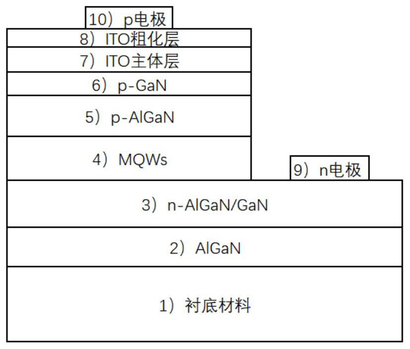
A kind of transparent electrode of light-emitting diode and preparation method thereof
A technology of light-emitting diodes and transparent electrodes, applied in circuits, electrical components, semiconductor devices, etc., can solve problems such as high cost and complicated process, achieve low absorption rate, avoid process treatment, and good current expansion effect
- Summary
- Abstract
- Description
- Claims
- Application Information
AI Technical Summary
Problems solved by technology
Method used
Image

Examples
Embodiment 1
[0041] Using existing MOCVD equipment, using organometallic trimethyl indium as indium source, organometallic tetrakis(dimethylamino)tin as tin source, oxygen with a purity of 99.9999% as oxygen source, argon as carrier gas and growth protection atmosphere, in Preparation of ITO transparent electrode on GaN-based ultraviolet 365nm LED.
[0042] The preparation method of the ITO transparent electrode of this embodiment is as follows:
[0043] S1. Pretreatment of gallium nitride-based LED epitaxial wafers: After cleaning the surface of gallium nitride-based ultraviolet 365nm LEDs with organic and inorganic acid and alkali, prevent contact with air and put them into the MOCVD reaction chamber as soon as possible. Then control the temperature at 600°C, control the pressure at 20 Torr, and process for 20 minutes.
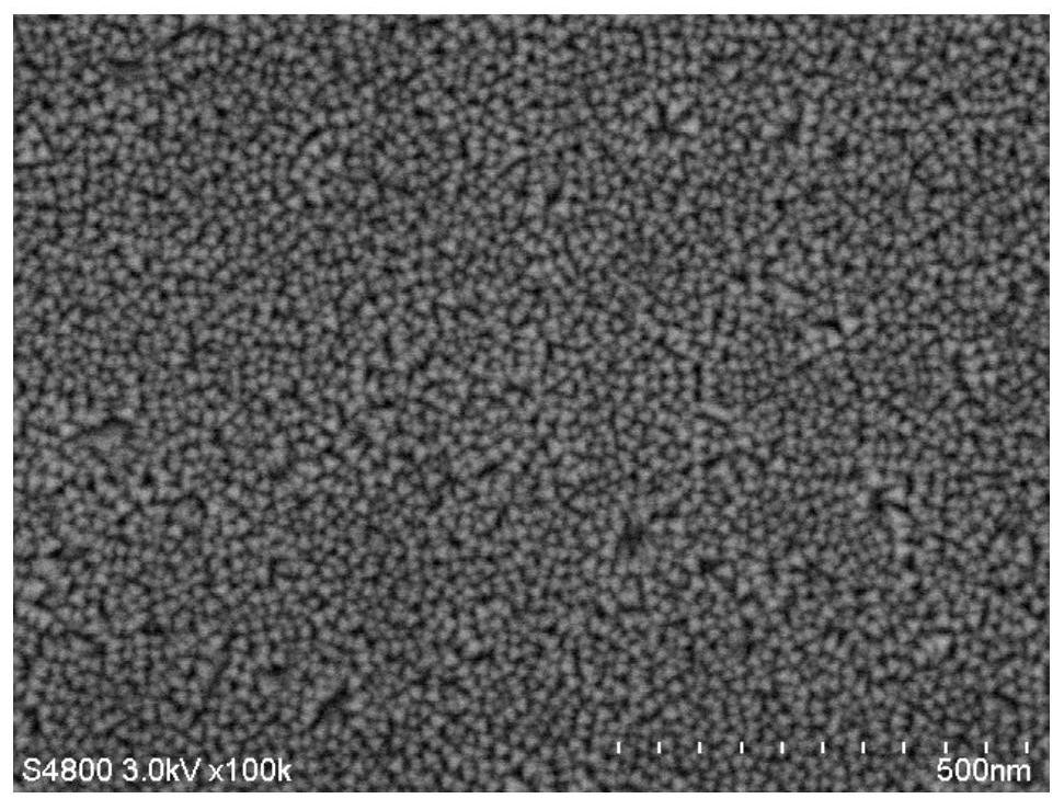
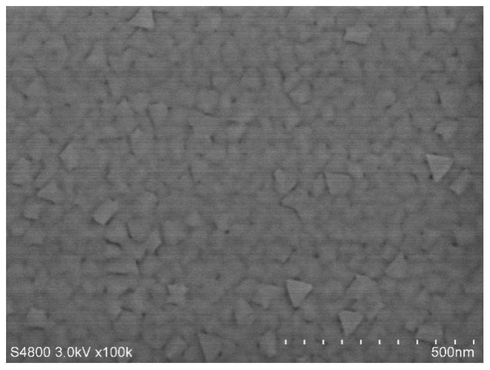
[0044] S2. ITO main layer growth: the growth temperature is controlled at 530°C, the pressure of the reaction chamber is controlled at 9Torr, and the indium source, oxy...
Embodiment 2
[0048] Utilizing the existing MOCVD equipment, using organometallic trimethyl indium as indium source, organic tetramethyl tin as tin source, oxygen with a purity of 99.9999% as oxygen source, argon as carrier gas and growth protection atmosphere, on gallium nitride based ITO transparent electrodes were prepared on ultraviolet 460nm LEDs.
[0049] The preparation method of the ITO transparent electrode of this embodiment is as follows:
[0050] S1. Pretreatment of gallium nitride-based LED epitaxial wafers: After cleaning the surface of gallium nitride-based ultraviolet 460nm LEDs with organic and inorganic acid and alkali, prevent contact with air and put them into the MOCVD reaction chamber as soon as possible. Then control the temperature at 700°C and the pressure at 10 Torr for 30 minutes.
[0051] S2. ITO main layer growth: the growth temperature is controlled at 600°C, the pressure of the reaction chamber is controlled at 6Torr, and the indium source, oxygen source and ...
Embodiment 3
[0055] Utilizing the existing MOCVD equipment, using organometallic trimethyl indium as indium source, organometallic tetraethyl tin as tin source, laughing gas as oxygen source, argon as carrier gas and growth protection atmosphere, in GaN-based ultraviolet 300nm LED ITO transparent electrodes were prepared on the top.
[0056] The preparation method of the ITO transparent electrode of this embodiment is as follows:
[0057] S1. Pretreatment of gallium nitride-based LED epitaxial wafers: After cleaning the surface of gallium nitride-based ultraviolet 300nm LEDs with organic and inorganic acid and alkali, prevent contact with air and put them into the MOCVD reaction chamber as soon as possible. Then control the temperature at 300°C and the pressure at 100 Torr for 1 min.
[0058] S2. ITO main layer growth: the growth temperature is controlled at 450 ° C, the pressure of the reaction chamber is controlled at 80 Torr, and the indium source, oxygen source and tin source are intr...
PUM
| Property | Measurement | Unit |
|---|---|---|
| thickness | aaaaa | aaaaa |
| wavelength | aaaaa | aaaaa |
Abstract
Description
Claims
Application Information