Insulated gate bipolar transistor

A technology of bipolar transistors and insulated gates, applied in semiconductor devices, electrical components, circuits, etc., can solve the problems of limiting the reliability of devices, the injection dose and energy cannot be large, and the injection energy is large

Inactive Publication Date: 2014-12-10
UNIV OF ELECTRONICS SCI & TECH OF CHINA +1
View PDF4 Cites 0 Cited by
  • Summary
  • Abstract
  • Description
  • Claims
  • Application Information

AI Technical Summary

Problems solved by technology

When the sum of the common base amplification factors of the two transistors is greater than 1, that is, α NPN +α PNP When ≥1, it will trigger the opening of the parasitic thyristor in the IGBT, and a latch-up effect will occur, causing the device to lose its gate control capability and cannot be turned off. temperature and positive safe operating area
[0004] A common method to improve the reliability of IGBT devices is to use a self-aligned process to form a P + The body region 6 is used to reduce the lateral resistance and the common base amplification factor of the parasitic NPN transistor in the P-type base region 5, but the P + The implant dose and energy of body region 6 should not be very large
If the implantation energy is too large, the masking effect of the polysilicon gate electrode 10 and the gate oxide 9 may fail; due to the self-alignment process for implantation, the implantation dose is too large, which may lead to P + The body region 6 extends seriously to the channel region, which will seriously affect the threshold voltage and turn-on energy of the device
This also limits the further improvement of device reliability by this method

Method used


Image

  • Insulated gate bipolar transistor
  • Insulated gate bipolar transistor
  • Insulated gate bipolar transistor

Examples


Embodiment Construction

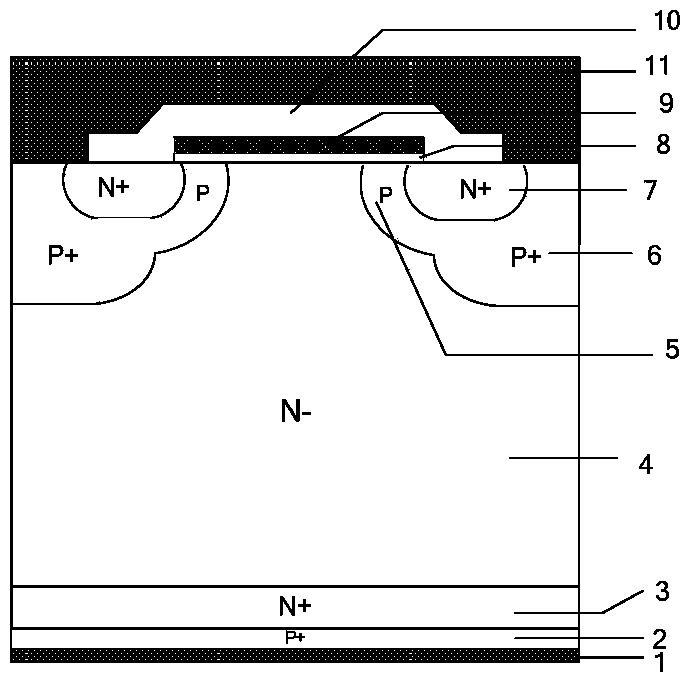
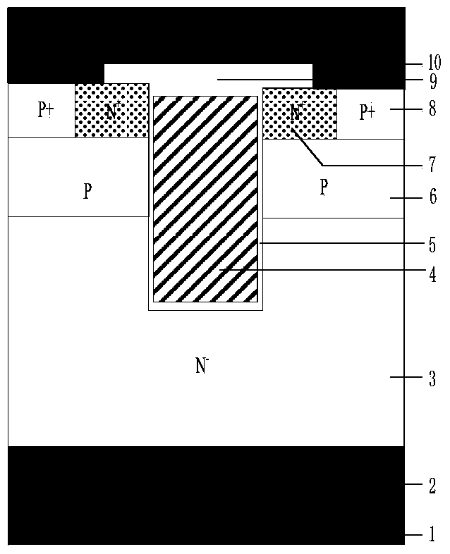
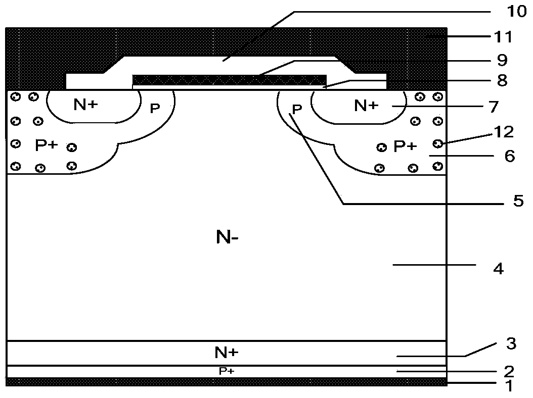
[0023] An insulated gate bipolar transistor, the structure of which is as follows image 3 , 4 As shown, including metallized collector 1, P-type collector 2, N + buffer layer 3, N - Drift zone 4, P + Body region 6, P-type base region 5, N + Source region 7, silicon dioxide gate oxide layer 8, polysilicon gate electrode 9, silicon dioxide field oxide layer 10, metallized emitter 11; metallized collector 1 is located on the back of the P-type collector region 2, N + The buffer layer 3 is located on the front of the P-type collector region 2, and the top is the same as the N - Drift zone 4 connected; N + source region 7 and P + The two body regions 6 are located side by side under the metallized emitter 12 and connected to the metallized emitter 12, wherein P + body region 6 below and N - Drift zone 4 is directly connected to the N + Source region 7 is the same as N - The drift region 4 is separated by a P-type base region 5; N - Drift region 4, P-type base region 5 a...


PUM


Abstract

The invention discloses an insulated gate bipolar transistor (IGBT), belonging to the technical field of power semiconductor devices. According to the invention, impurities in a deep energy level (12) with an acceptor level are introduced into a P+ conductor region (6) of the traditional insulated gate bipolar transistor through an ion implantation or impurity diffusion manner. At the room temperature, only a small part of the impurities in the deep energy level (12) imported into the P+ conductor region (6) are ionized, so that the impact on the positive conduction work of the device can be ignored. When large current flows inside the device and the heat loss of the device increases, the ionization rate of the impurities in the deep energy level (12) can increase along with the rising temperature of the device, so that the effective doping concentration of a base region of an NPN tube in a parasitic NPNP thyristor structure in the IGBT device can be increased, the injection efficiency gamma of an emitter of the NPN tube can be reduced, then, the amplification coefficient alpha NPN of a common base of the NPN tube can be reduced, and the consequence that the parasitic thyristor of the device is opened when alpha NPN plus alpha PNP is more than or equal to 1 so that the device can be finally burnt out for the device cannot be turned off due to the loss of grid control ability can be avoided, thereby finally achieving the purpose of enlarging the positive safety work area of the device and improving the reliability of the device.

Description

technical field [0001] The invention belongs to the technical field of power semiconductor devices, and relates to an insulated gate bipolar transistor (IGBT) device structure and a preparation method thereof. Background technique [0002] Insulated gate bipolar transistor (IGBT) is a new type of power semiconductor device. It not only has the advantages of high input impedance, low driving power, simple driving circuit and high switching speed of MOSFET, but also has the advantages of high current density, low saturation voltage and strong current handling ability of bipolar transistor. Therefore, IGBT has three characteristics of high voltage, high current and high speed, which are unmatched by other power devices. As a power switching tube or power output tube, IGBT is widely used in induction cooker, UPS uninterruptible power supply, automotive electronic igniter, three-phase motor inverter, welding machine switching power supply and other products, and has become one o...

Claims


Application Information

Patent Timeline
Patent Type & Authority Patents(China)
IPC IPC(8): H01L29/06H01L29/739
Inventor 李泽宏赵起越李巍任敏张金平张波
Owner UNIV OF ELECTRONICS SCI & TECH OF CHINA
Why Eureka
Try Eureka