Substrate connector

a connector and substrate technology, applied in the direction of coupling contact members, coupling device connections, printed circuits, etc., can solve the problems of increasing costs and the inability to replace the terminal b>810/b> with a new terminal, so as to improve reliability, reduce costs, and simplify the structure

Inactive Publication Date: 2012-08-07
MOLEX INC
View PDF10 Cites 0 Cited by
  • Summary
  • Abstract
  • Description
  • Claims
  • Application Information

AI Technical Summary

Benefits of technology

[0006]An object of the present invention therefore is to solve the above-mentioned problems encountered by the conventional substrate connector through provision of a reliable substrate connector in which a concave part provided in the terminal and is engaged with a convex part received in a terminal-receiving cavity formed so as to penetrate a plate-like housing, so that the terminal is held in the cavity and is permitted to vertically and laterally move therein, thereby absorbing variations in the space defined between the connector and the substrate while maintaining a reliable electric contact with the substrate, reducing the cost through a simplified structure, and permitting easy replacement of a terminal.
[0011]In accordance with a further embodiment of the present invention, there is provided a substrate connector, with a mounting portion having an upper convex portion and a lower convex portion protruding outward from an outer edge thereof to define the concave portion, and wherein a lower side of the lower convex portion closer to the first substrate contacts a convex part while inserted into the broad width part thus causing the bifurcated portion of the terminal to be elastically deformed and inwardly tilted.
[0013]According to the present invention, the concave portion formed in the terminal engages the convex part formed in the housing cavity thereby permitting the terminal to be held so that it moves vertically and laterally in the cavity. Hence, variations in space between the substrate connector and a substrate are appropriately absorbed while maintaining contact with the substrate, reducing costs through a simplified structure, and allowing replacement of the terminal as required thereby enhancing the reliability.

Problems solved by technology

Additionally, because the upper and lower housings 803,805 are joined together to form the housing 801, the assembly process becomes complicated, resulting in an increase in cost.
Furthermore, the terminal 810 cannot be removed from the housing 801, and thus the damaged terminal 810 cannot be replaced with a new terminal.

Method used


Image

  • Substrate connector
  • Substrate connector
  • Substrate connector

Examples


Embodiment Construction

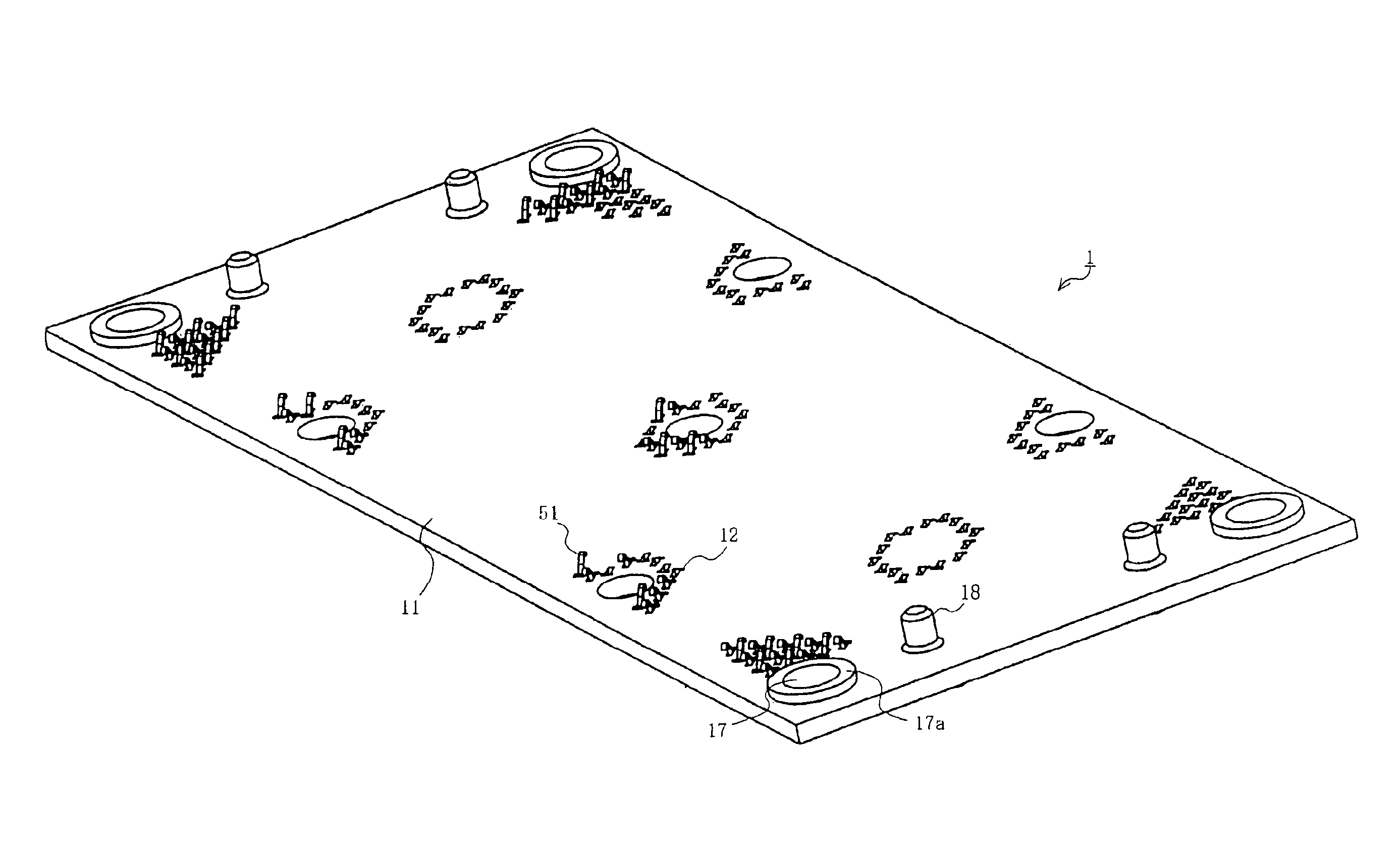
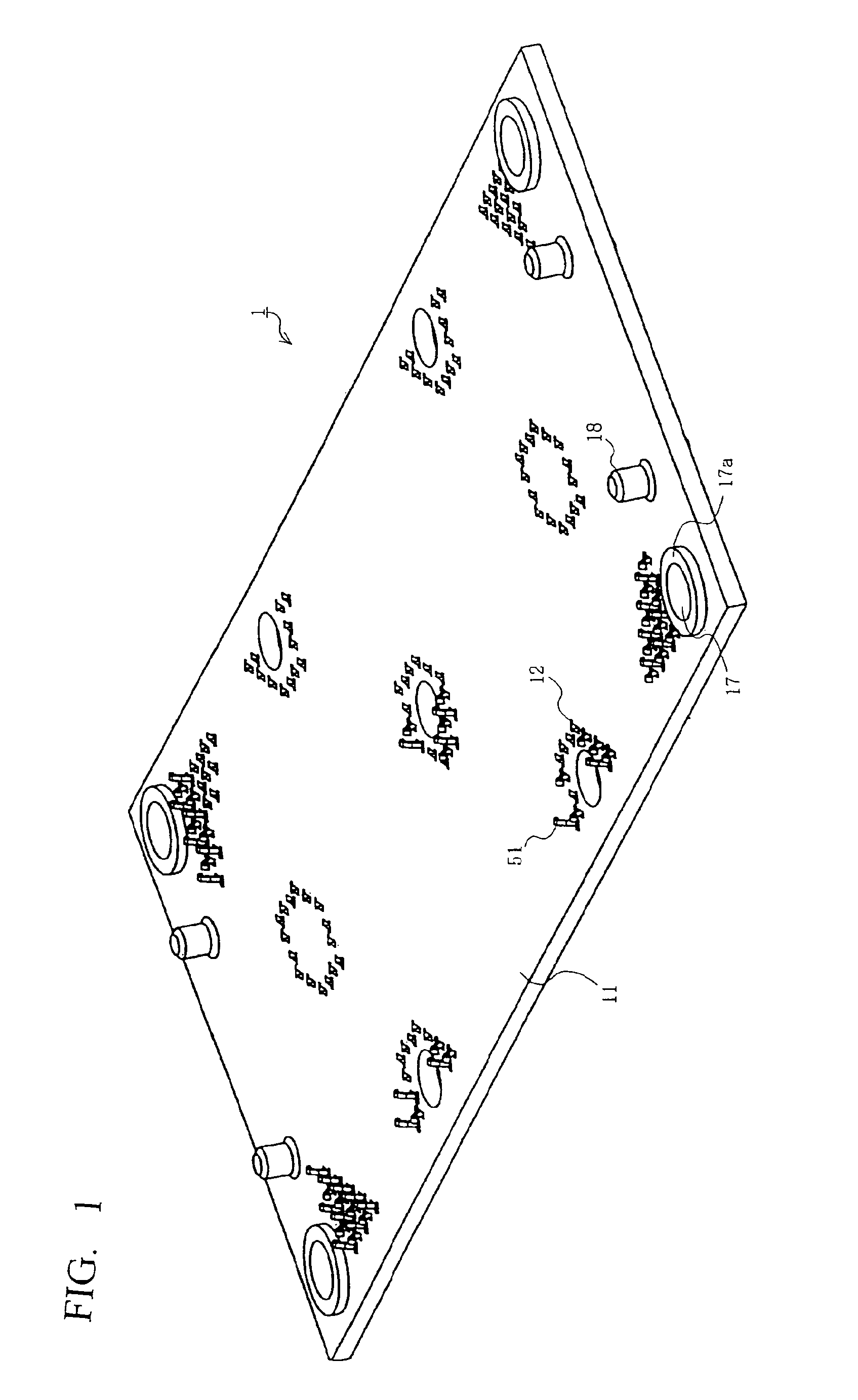
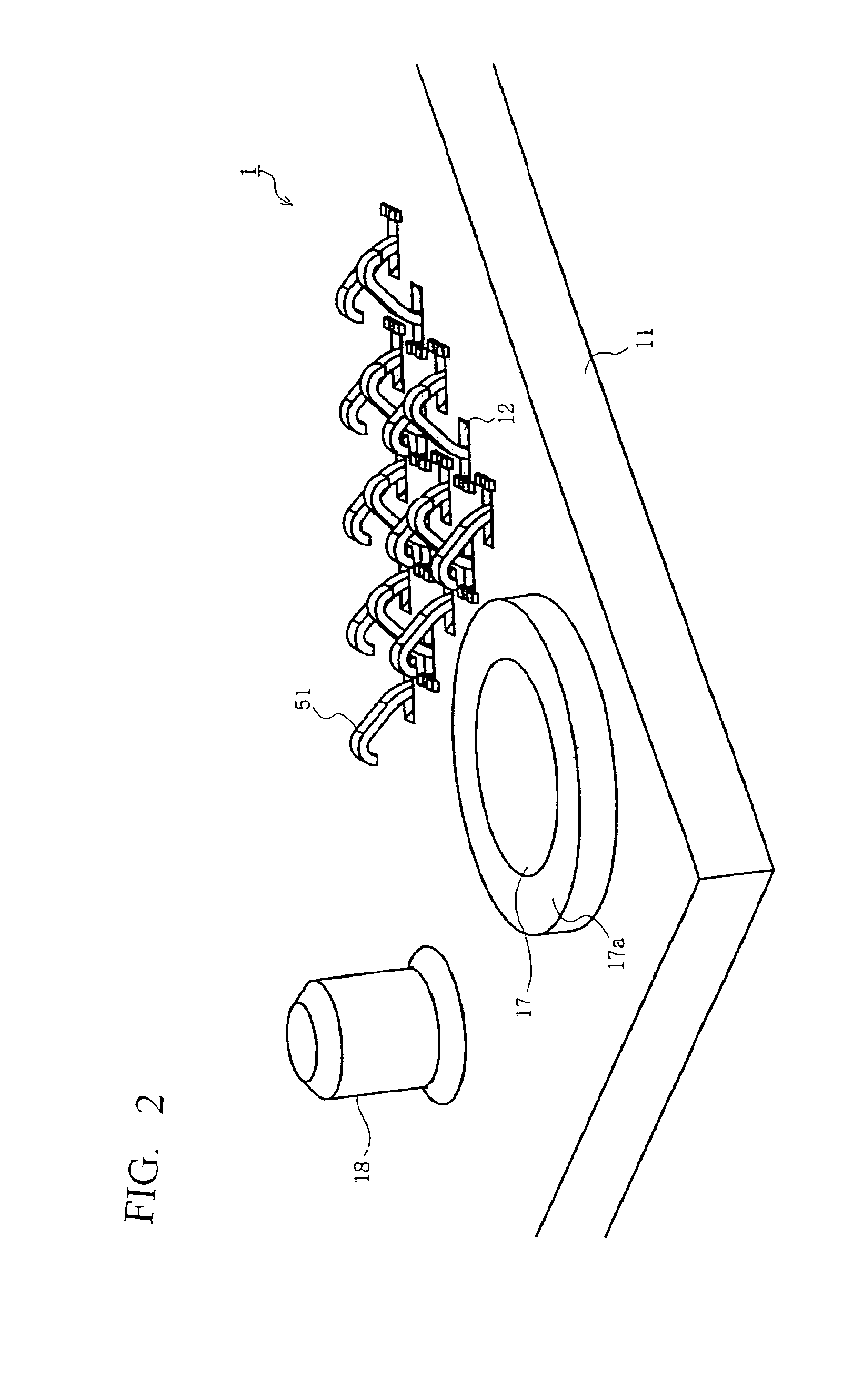
[0027]Referring to the drawings, 1 represents a connector used as a substrate connector. The connector 1 has a rectangular housing 11. The housing 11 is used between a first substrate 111 and a second substrate 121 in such manner that one surface thereof is opposed to a surface of the first substrate 111 (FIG. 3) on which first contact pads 113 are arranged and the other surface thereof is opposed to a surface of the second substrate 121 on which second contact pads 123 are arranged. (FIG. 4.) Thus, the housing 11 provides continuity between the first contact pads 113 of the first substrate 111 and the second contact pads 123 of the second substrate 121.

[0028]The first substrate 111 and the second substrate 121 are, for example, circuit boards such as printed circuit boards used in various types of electronic devices. The first substrate 111 or the second substrate 121 may also include a semiconductor device such as an IC or LSI , or any type of electronic device as long as it inclu...


PUM


Abstract

A substrate connector utilizes a plurality of conductive terminals, each of which are held in a single terminal-receiving cavity of a substrate. The terminals of the connector have a hook-shape with a retention portions in the form of a fork having a central slot and two free ends spaced apart from the retention portion and which protrude out of their cavities for contacting contact pads on opposing circuit boards. The retention portions engage abutments formed in the cavities to hold the terminals in place but do so in a manner that permits the terminals to move in both the vertical and horizontal directions.

Description

BACKGROUND OF THE INVENTION[0001]The present invention relates generally to a substrate connector, and more particularly to substrate connector with improved contact force characteristics.[0002]Conventional flat connectors that use a large number of terminals are used to connect a semiconductor device to a circuit board or to connect two substrates with each other. An example is shown in Japanese Patent Application Laid-Open (Kokai) No. 08-222335). FIG. 13 is a cross-sectional view of a conventional connector.[0003]In FIG. 13, 801 represents a connector housing that has an upper housing 803 with an opening 804 and a lower housing 805 with a bore 806. 810 is a connector terminal provided with a base 811 mounted in the bore 806, a contact arm 813 that is bent from the base 811 and extending upward, and a contact part 812 protruding downward from the lower end of the base portion 811. When the terminal 810 is inserted into the bore 806 from above, the lower end of a wing 815 protrudes ...

Claims


Application Information

Patent Timeline
Patent Type & Authority Patents(United States)
IPC IPC(8): H01R12/00H01R12/71
CPCH01R13/2442H01R12/714H01R13/432H01R13/24
Inventor ADACHI, KIYOSHI
Owner MOLEX INC
Why Eureka
Try Eureka