Method for air gap interconnect integration using photo-patternable low k material

a low-k material and air gap technology, applied in the field of air gapcontaining metalinsulator interconnect structures, can solve the problems of affecting the propagation of information, affecting the reliability of interconnect structures, and damage to metal lines by isotropic etching steps, etc., and achieves high-reliability interconnect structures.

Active Publication Date: 2012-08-14
ALSEPHINA INNOVATIONS INC
View PDF55 Cites 284 Cited by
  • Summary
  • Abstract
  • Description
  • Claims
  • Application Information

AI Technical Summary

Benefits of technology

[0007]The present invention relates to methods for producing air gap-containing metal-insulator interconnect structures for VLSI and ULSI devices using a photo-patternable low k (PPLK) material as well as the air gap-containing interconnect structure formed thereby. More particularly, the methods described herein provide interconnect structures built in a photo-patternable low k material in which air gaps are defined by photolithography in the photo-patternable low k material. In the methods of the present invention, no etch step is required to form the air gaps. Since no etch step is required in forming the air gaps within the photo-patternable low k material, the methods disclosed in this invention provide highly reliable interconnect structures.

Problems solved by technology

Interconnect structures in integrated circuits induce a delay in the propagation of the information between semiconductor devices such as transistors.
There are several problems with the aforementioned prior art air gap fabrication scheme.
If the lithography step is not perfect (misalignment, or too large an opening may result) and, if the etch step leads to a width increase, the metal lines can be damaged by this etch step.
The isotropic etch process may also damage the sidewalls of the metal line or the interface between the metal lines and an overlying cap layer.
Both issues may lead to reliability issues.
Finally, the need for very high resolution lithography and a critical etch step leads to a huge increase in the cost of the air gap module.

Method used


Image

  • Method for air gap interconnect integration using photo-patternable low k material
  • Method for air gap interconnect integration using photo-patternable low k material
  • Method for air gap interconnect integration using photo-patternable low k material

Examples


Embodiment Construction

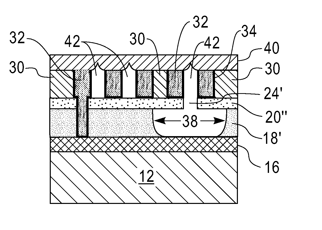
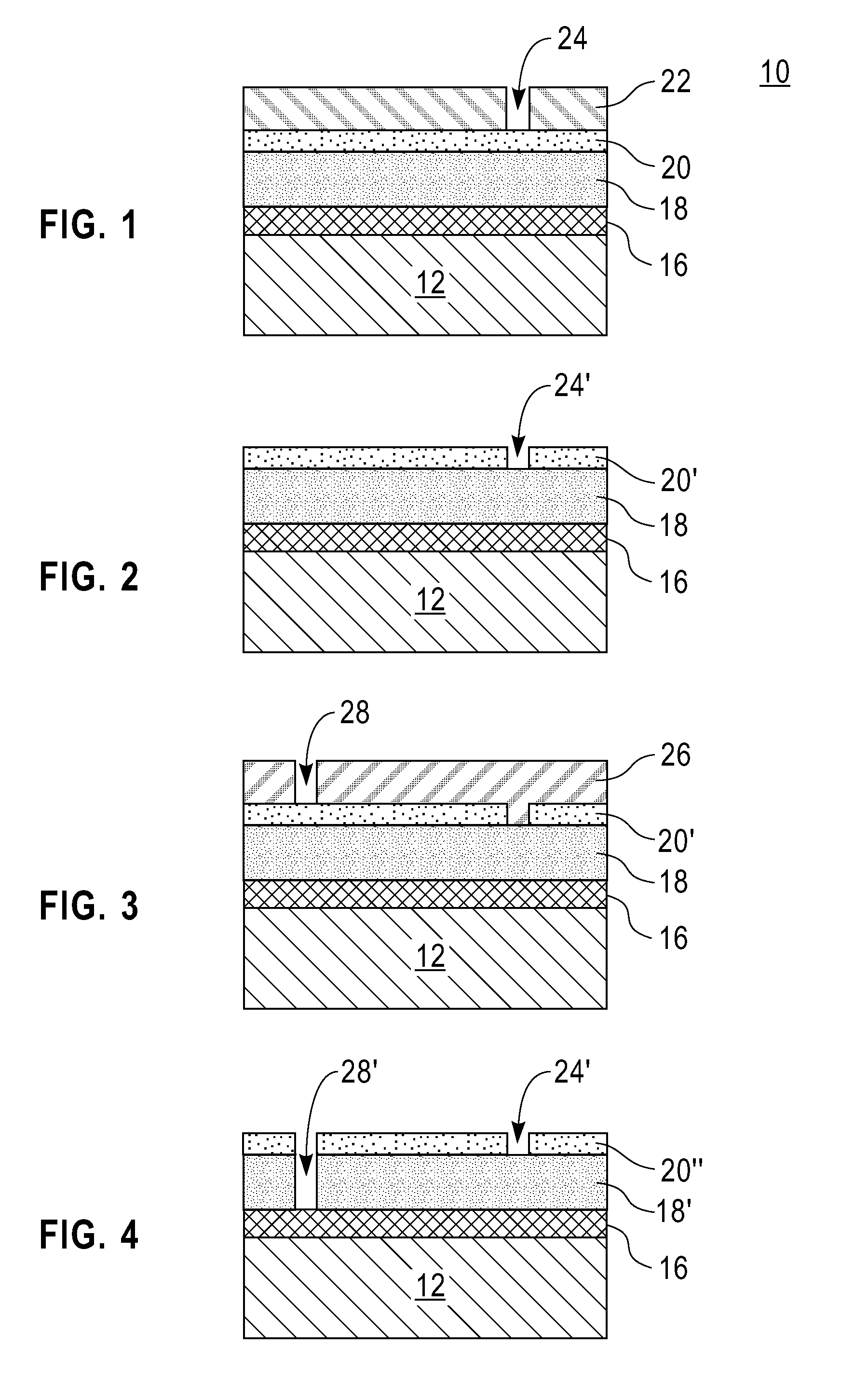
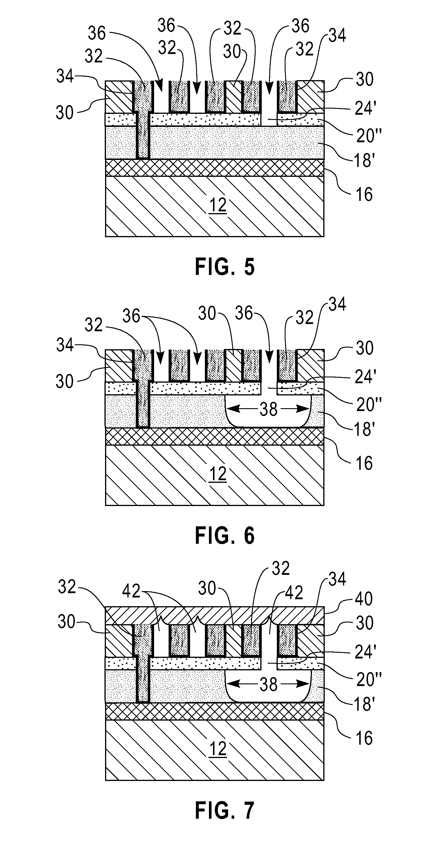
[0026]The present invention, which provides air gap-containing interconnect structures and methods of fabricating such air gap-containing interconnect structures, will now be described in greater detail by referring to the following discussion and drawings that accompany the present application. It is observed that the drawings of the present application are provided for illustrative purposes and, as such, the drawings are not drawn to scale.

[0027]In the following description, numerous specific details are set forth, such as particular structures, components, materials, dimensions, processing steps and techniques, in order to provide an understanding of some aspects of the present invention. However, it will be appreciated by one of ordinary skill in the art that the invention may be practiced without these specific details. In other instances, well-known structures or processing steps have not been described in detail in order to avoid obscuring the invention.

[0028]It will be under...


PUM


Abstract

Methods for producing air gap-containing metal-insulator interconnect structures for VLSI and ULSI devices using a photo-patternable low k material as well as the air gap-containing interconnect structure that is formed are disclosed. More particularly, the methods described herein provide interconnect structures built in a photo-patternable low k material in which air gaps are defined by photolithography in the photo-patternable low k material. In the methods of the present invention, no etch step is required to form the air gaps. Since no etch step is required in forming the air gaps within the photo-patternable low k material, the methods disclosed in this invention provide highly reliable interconnect structures.

Description

RELATED APPLICATIONS[0001]This application is related to co-pending and co-assigned U.S. application Ser. No. 12 / 721,032, entitled “METHODS FOR FABRICATION OF AN AIR GAP-CONTAINING INTERCONNECT STRUCTURE” filed Mar. 10, 2010, and co-pending and co-assigned U.S. application Ser. No. 12 / 768,267, entitled “STRUCTURES AND METHODS FOR AIR GAP INTEGRATION” filed Apr. 27, 2010, the entire contents of which are both incorporated herein by reference.FIELD OF THE INVENTION[0002]The present invention relates to air gap-containing metal-insulator interconnect structures for Very Large Scale Integrated (VLSI) and Ultra-Large Scale Integrated (ULSI) devices and methods of forming the same.BACKGROUND OF THE INVENTION[0003]Interconnect structures in integrated circuits induce a delay in the propagation of the information between semiconductor devices such as transistors. To reduce this delay, the interconnect structures should posses the lowest capacitance possible. One approach to form interconnec...

Claims


Application Information

Patent Timeline
Patent Type & Authority Patents(United States)
IPC IPC(8): H01L21/76H01L21/4763H01L21/44
CPCH01L21/02126H01L21/02274H01L21/02282H01L21/02318H01L21/31H01L21/3105H01L21/76807H01L21/7682H01L21/76825H01L21/76826H01L21/76828H01L21/76829H01L21/76835H01L23/5222H01L23/53295H01L2221/1031H01L2221/1036H01L2924/12044H01L2924/0002H01L2924/00
Inventor CLEVENGER, LAWRENCE A.DARNON, MAXIMELIN, QINGHUANGLISI, ANTHONY D.NITTA, SATYANARAYANA V.
Owner ALSEPHINA INNOVATIONS INC
Why Eureka
Try Eureka