Liquid crystal display device

a display device and liquid crystal technology, applied in static indicating devices, instruments, non-linear optics, etc., can solve problems such as non-uniform brightness of screens, and achieve the effect of reducing the delay difference of gate signals and uniform brightness

Active Publication Date: 2012-08-21
SAMSUNG DISPLAY CO LTD
View PDF10 Cites 2 Cited by
  • Summary
  • Abstract
  • Description
  • Claims
  • Application Information

AI Technical Summary

Benefits of technology

[0010]Accordingly, it is an aspect of the present invention to provide an LCD device having more uniform brightness through reduction in the delay difference of the gate signals.

Problems solved by technology

The level of the kickback voltage varies depending on the delay of the gate signals, thereby making the brightness of the screen non-uniform.

Method used


Image

  • Liquid crystal display device
  • Liquid crystal display device
  • Liquid crystal display device

Examples


Embodiment Construction

[0045]In the following description, if a layer is said to be formed ‘on’ another layer, then a third layer may be disposed between the two layers or the two layers may be contacted with each other. In other words, it will be understood that when an element such as a layer, film, region, or substrate is referred to as being “on” another element, it can be directly on the other element or intervening elements may also be present. Further, a layer is said to be formed ‘right on’ another layer, it will be understood that the two layers contact with each other.

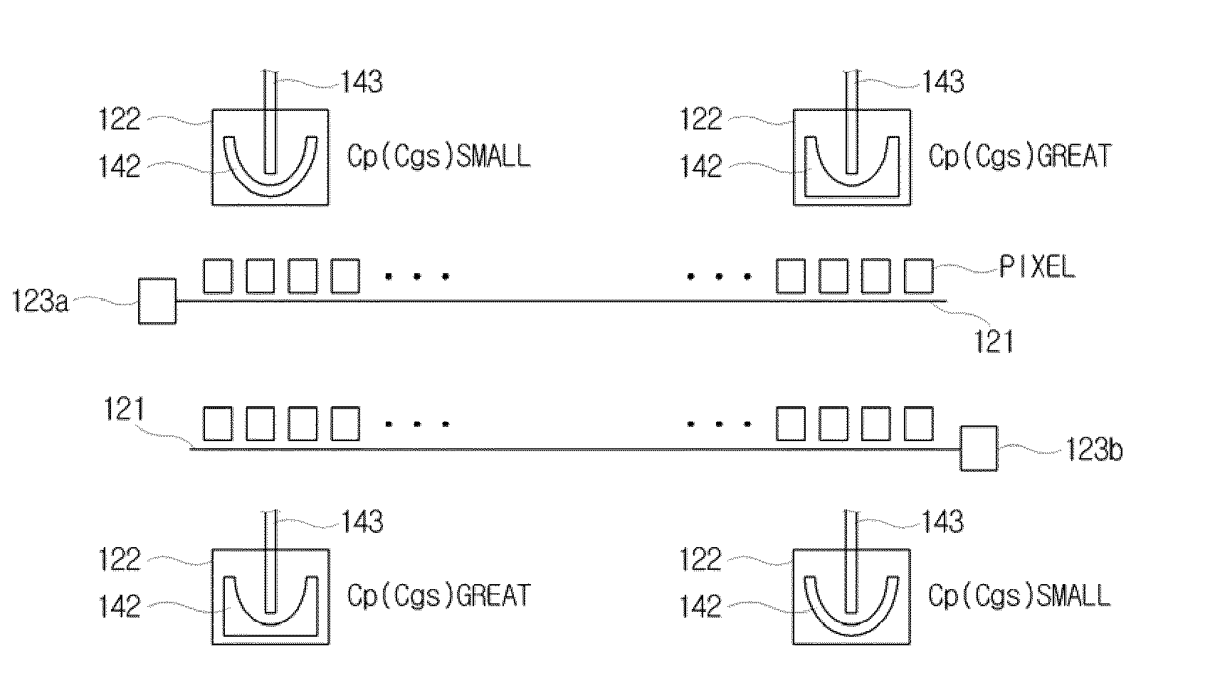
[0046]It should be noted that a pixel unit refers to a unit to display a screen where different colors of light from a plurality of pixels are mixed to provide light with desired color and brightness. For example, a red pixel, a blue pixel, and a green pixel form into one pixel unit.

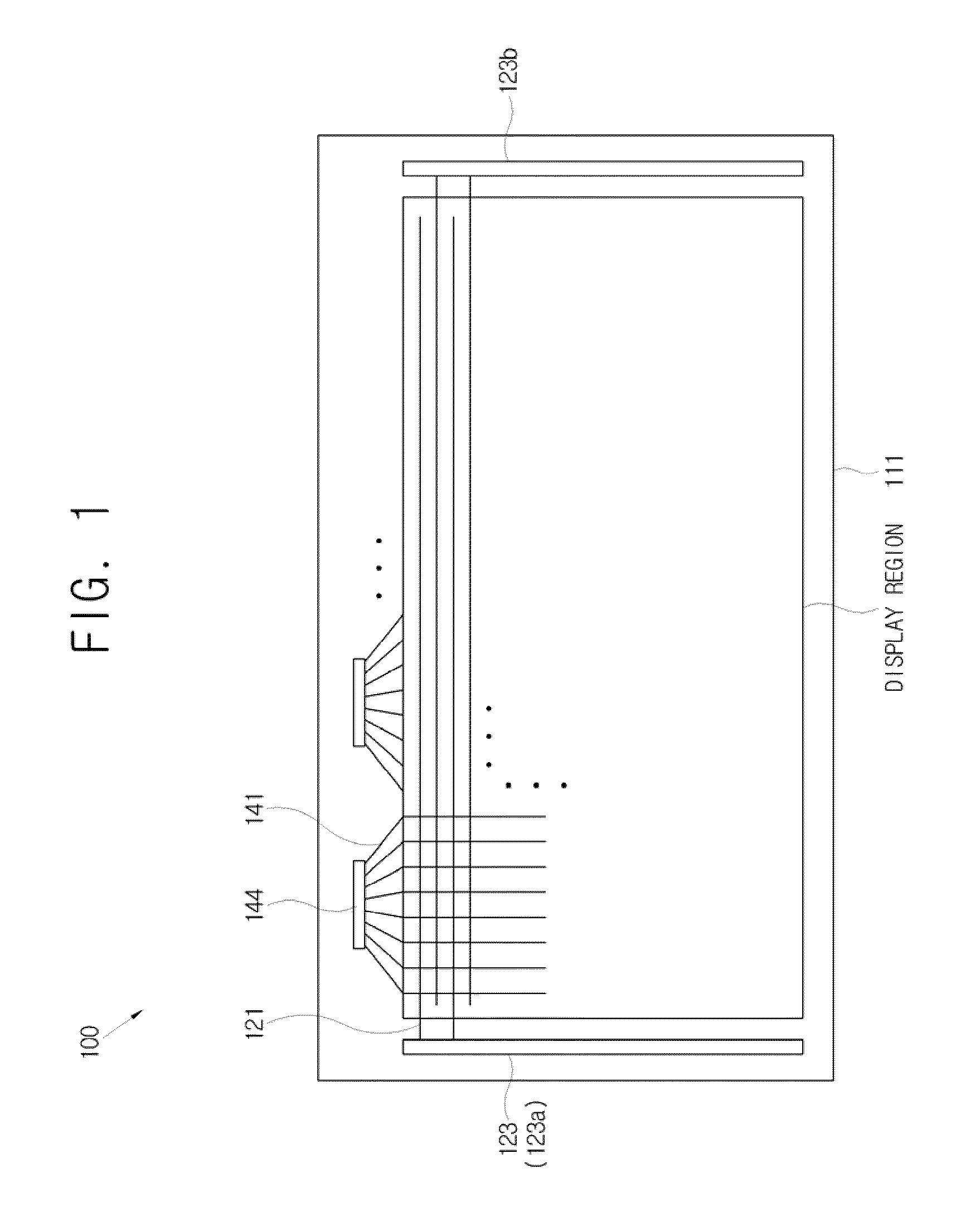
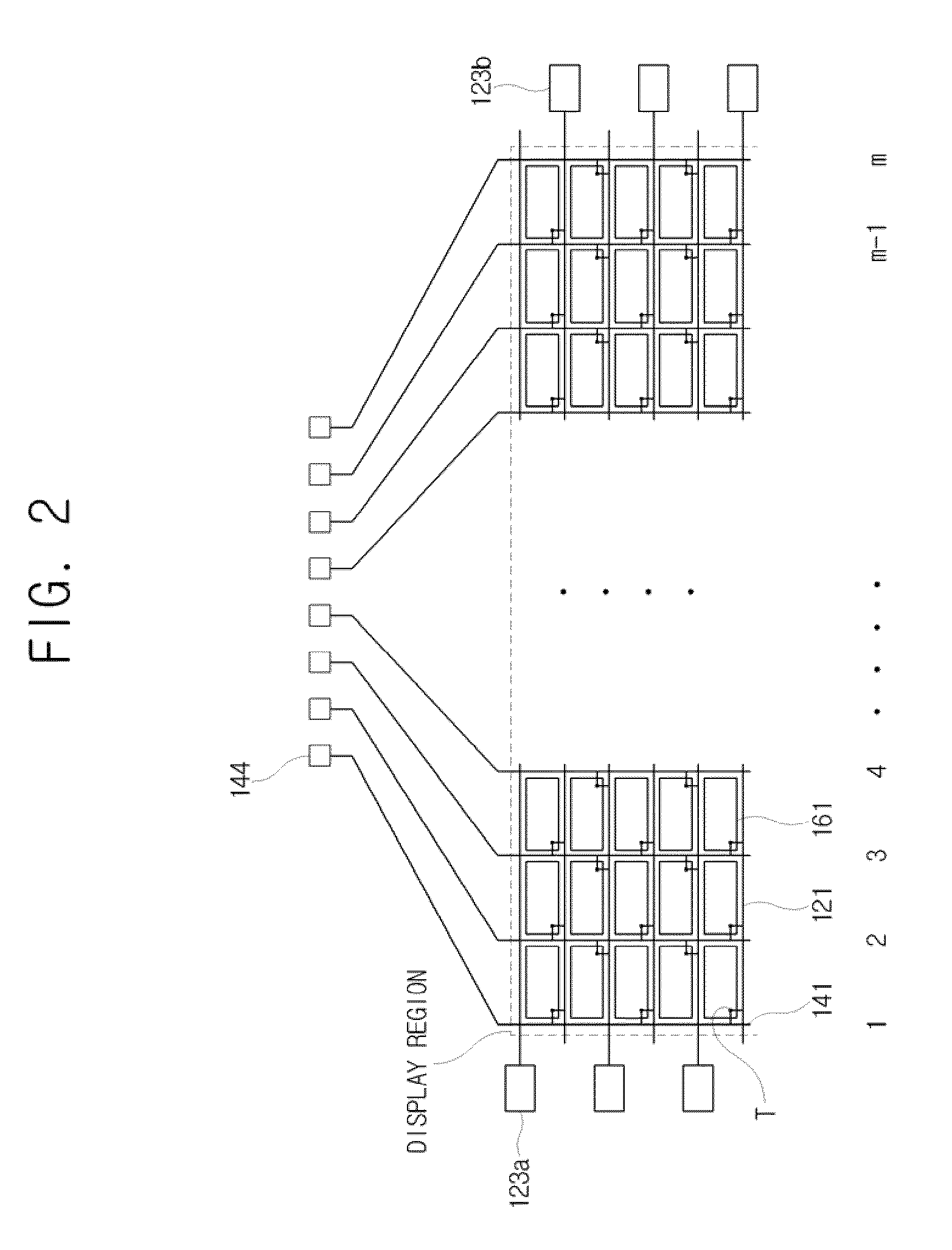
[0047]Hereinafter, an LCD device according to exemplary embodiments of the present invention will be described with reference to FIGS. 1 through 5

[0048...


PUM

PropertyMeasurementUnit
kickback voltageaaaaaaaaaa

Abstract

A liquid crystal display device includes a first substrate which comprises a plurality of pixels where a thin film transistor and a pixel electrode electrically connected to the thin film transistor are formed, the first substrate including a gate line and a data line which insulatingly intersect each other; and a gate driver which applies a gate driving signal to the gate line, the thin film transistor including a gate electrode which is connected to the gate line; a source electrode which is connected to the data line; and a drain electrode which is connected to the pixel electrode, and the pixels being decreased in a value of Cp / (Cp+Clc+Cst) as going toward the gate driver (where, Cp: a sum of parasitic capacity between the gate electrode and the source electrode and parasitic capacity between the gate electrode and the drain electrode, Clc: liquid crystal capacity, and Cst: storage capacity).

Description

CROSS-REFERENCE TO RELATED APPLICATIONS[0001]This application is a continuation of U.S. patent application Ser. No. 11 / 781,112, filed Jul. 20, 2007, which claims priority upon Korean Patent Application No. 2006-0086747, filed on Sep. 8, 2006 in the Korean Intellectual Property Office, the disclosure of which is incorporated herein by reference.BACKGROUND OF INVENTION[0002]1. Field of Invention[0003]Apparatuses and methods consistent with the present invention relate to a liquid crystal display device.[0004]2. Description of the Related Art[0005]A liquid crystal display (LCD) device includes a first substrate where thin film transistors are formed, a second substrate which is disposed opposite to the first substrate, and a liquid crystal layer disposed between the two substrates.[0006]Gate lines and data lines are formed on the first substrate and insulatingly intersect intersect each other to form pixels. The pixels are connected to the thin film transistors. When the gate lines rec...

Claims


Application Information

Patent Timeline
Patent Type & Authority Patents(United States)
IPC IPC(8): G02F1/136G02F1/1343G02F1/1345
CPCG02F1/1393G09G3/3648G02F1/136213G09G2320/0223G09G2320/0219G02F1/133G02F1/1343
Inventor LEE, MIN-CHEOL
Owner SAMSUNG DISPLAY CO LTD
Why Eureka
Try Eureka