Eureka AIR delivers breakthrough ideas for toughest innovation challenges, trusted by R&D personnel around the world.

Buried layer of an integrated circuit

a technology of integrated circuits and layers, applied in the direction of basic electric elements, electrical apparatus, semiconductor devices, etc., can solve the problems of crystalline defects, insufficient protection effect of sacrificial oxide, and insufficient transit of consumed semiconductor materials, so as to reduce the downside of implantation

Active Publication Date: 2012-09-04
MACRONIX INT CO LTD
View PDF11 Cites 2 Cited by
  • Summary
  • Abstract
  • Description
  • Claims
  • Application Information

AI Technical Summary

Benefits of technology

[0005]The described technology reduces the downside of implantation by disposing of an amount of the crystal lattice which was damaged during implantation.
[0009]after removing the sacrificial oxide, growing a pre-anneal oxide consuming part of the intermediate region of the semiconductor material transited by the implanted first charge type dopants. When pre-anneal oxide is grown, such as silicon oxide on silicon, part of the silicon substrate is consumed in the chemical reaction. As with the prior sacrificial oxide, this consumed semiconductor material had also been transited by, and damaged by, the implanted dopants. Accordingly, growing the pre-anneal oxide helps to remove semiconductor material with a damaged crystalline lattice.
[0010]annealing the first charge type buried layer covered by the pre-anneal oxide. Annealing activates the implanted dopants by helping to move the implanted dopants into appropriate locations of the crystalline lattice.
[0046]wherein the n-type buried layer lowers a resistance of said at least one of the source and drain regions formed in the n-type well.

Problems solved by technology

Unfortunately, as the energetic dopants penetrate the substrate material damage to the crystalline structure results.
Collisions with the nuclei of the substrate material knock the substrate nuclei out of the crystalline lattice, resulting in crystalline defects.
If the sacrificial oxide were absent, the implanted dopants would have passed through and damaged the semiconductor crystalline lattice instead.
The damage would otherwise have occurred in the semiconductor crystalline lattice.
As with the prior sacrificial oxide, this consumed semiconductor material had also been transited by, and damaged by, the implanted dopants.
Below 50 angstroms, it is believed that the sacrificial oxide is too thin to provide a substantial protective effect against implantation damage.
Above 300 angstroms, it is believed that the energies required to implant the ions to sufficient depth become impractically high.

Method used


Image

  • Buried layer of an integrated circuit
  • Buried layer of an integrated circuit
  • Buried layer of an integrated circuit

Examples


Embodiment Construction

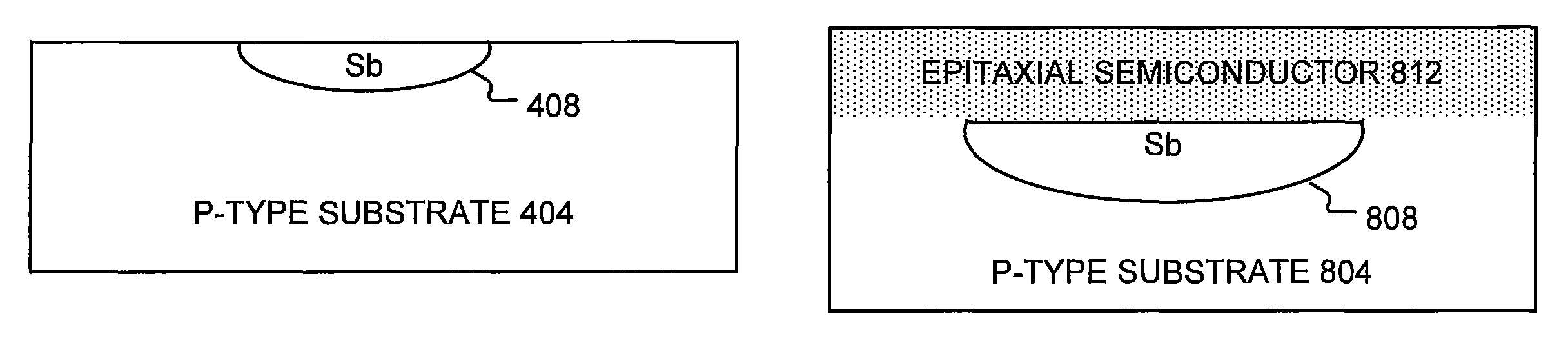
[0093]An n-type buried layer in a p-type substrate generally isolates the p-type substrate from the p-type well. An n-type buried layer in a p-type substrate also reduces resistance of an n-well in a p-type substrate.

[0094]A p-type buried layer in an n-type substrate generally isolates the n-type substrate from the n-type well. A p-type buried layer in an n-type substrate also reduces resistance of a p-well in an n-type substrate.

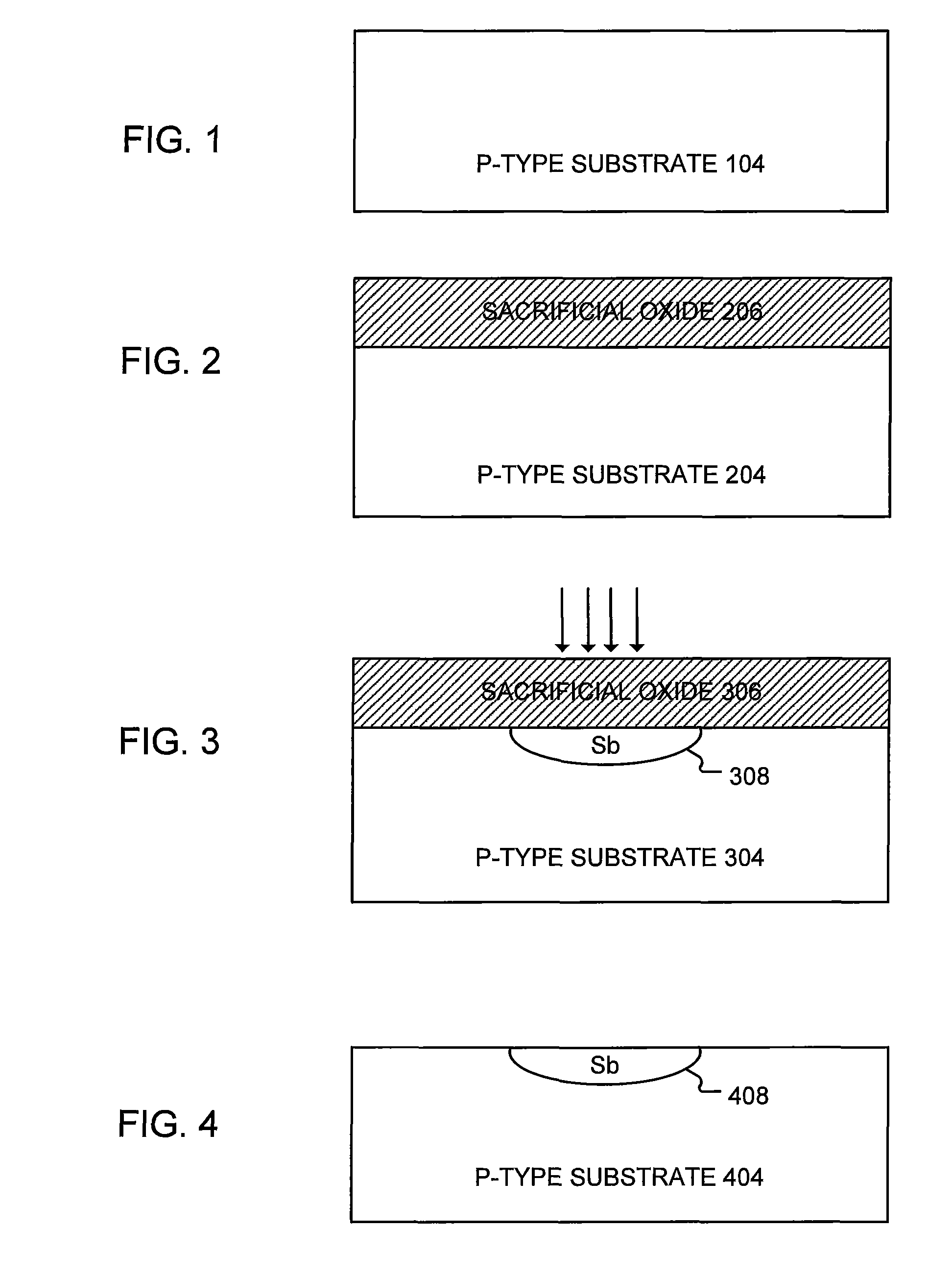
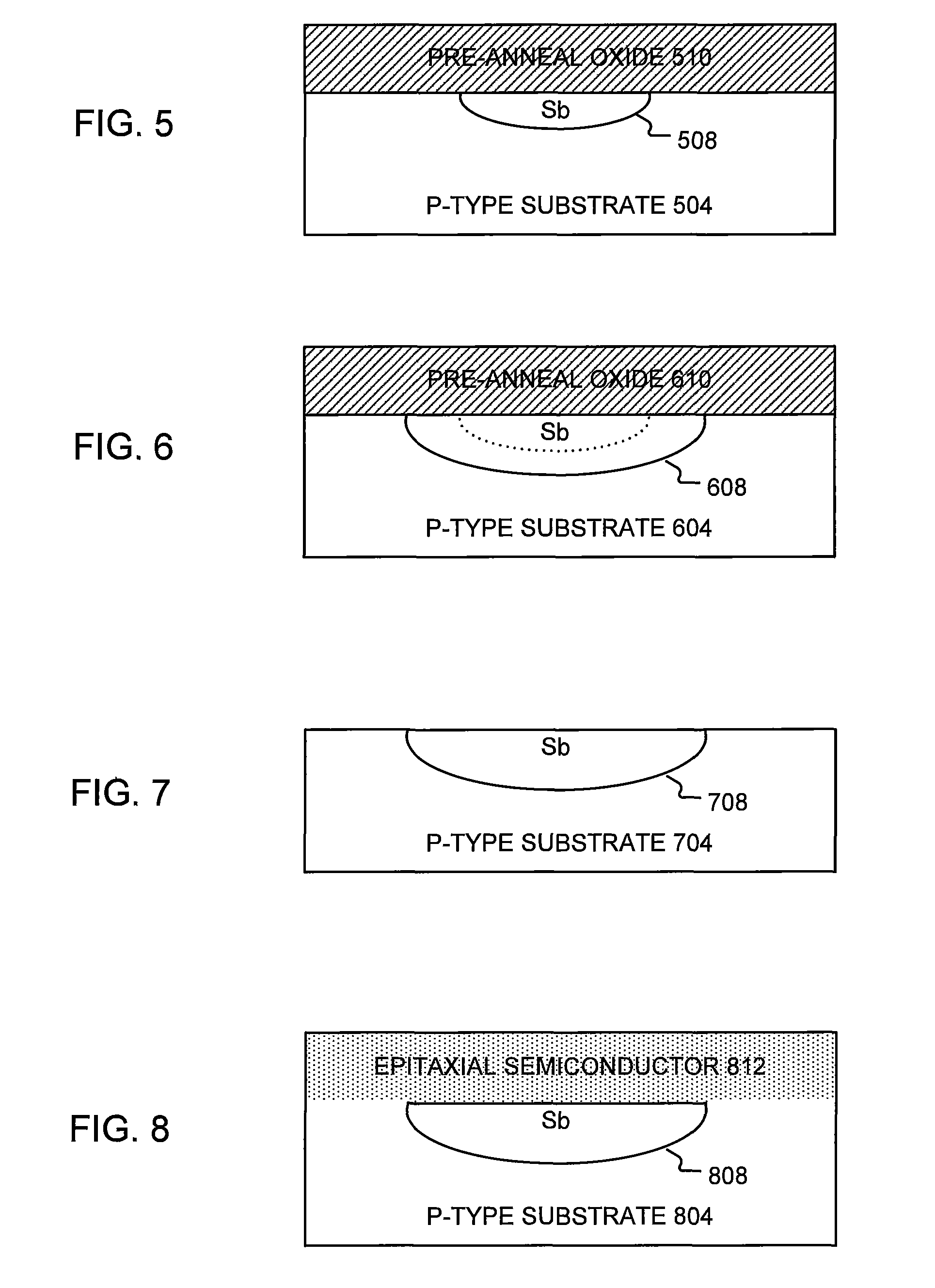
[0095]FIGS. 1-8 show a process flow of making an n-type buried layer on a p-type substrate.

[0096]FIG. 1 shows a p-type substrate 104 on which the n-type buried layer is grown. A p-type epitaxial layer over a substrate is also considered a type of p-type substrate.

[0097]FIG. 2 shows the formation of a sacrificial oxide 206 on the p-type substrate 204.

[0098]The sacrificial oxide is made with a thickness of between about 50 and 300 angstroms. Below 50 angstroms, it is believed that the sacrificial oxide is too thin to provide a substantial protective effect ag...


PUM


Abstract

Various aspects of the technology are directed to integrated circuit manufacturing methods and integrated circuits. In one method, a first charge type buried layer in a semiconductor material of an integrated circuit by implanting first charge type dopants of the first charge type buried layer through a sacrificial oxide over the semiconductor material and through an intermediate region of the semiconductor material transited by the implanted first charge type dopants. When the implanted dopants pass through the sacrificial oxide, damage to the semiconductor crystalline lattice is averted. If the sacrificial oxide were absent, the implanted dopants would have passed through and damaged the semiconductor crystalline lattice instead. Later, a pre-anneal oxide is grown and removed.

Description

BACKGROUND[0001]1. Field of the Invention[0002]The described technology relates to forming a n-type or p-type buried layer with few defects in an integrated circuit.[0003]2. Description of Related Art[0004]Implantation of dopants is a more accurate alternative to diffusion. Unfortunately, as the energetic dopants penetrate the substrate material damage to the crystalline structure results. Collisions with the nuclei of the substrate material knock the substrate nuclei out of the crystalline lattice, resulting in crystalline defects. Accordingly, the use of implantation technology is a tradeoff of more precise doping in exchange for damage to the semiconductor crystal structure.SUMMARY[0005]The described technology reduces the downside of implantation by disposing of an amount of the crystal lattice which was damaged during implantation.[0006]One aspect of the technology is an integrated circuit manufacturing method, comprising:[0007]making a first charge type buried layer in a semic...

Claims


Application Information

Patent Timeline
Patent Type & Authority Patents(United States)
IPC IPC(8): H01L21/76
CPCH01L21/2652H01L21/324H01L21/761H01L29/0821H01L29/107H01L29/167H01L29/66272H01L29/7322H01L29/78
Inventor HUANG, YIN-FUCHANG, MING RONGLIEN, SHIH-CHIN
Owner MACRONIX INT CO LTD
Why Eureka
Eureka Blog
Learn More