Structure of high-frequency components with low stray capacitances

a technology of high-frequency components and capacitances, applied in the direction of diodes, transistors, electrical devices, etc., can solve the problem that the capacitance is not negligible in certain cases, and achieve the effect of reducing the stray capacitance between components

Active Publication Date: 2012-09-18
STMICROELECTRONICS SRL
View PDF11 Cites 0 Cited by
  • Summary
  • Abstract
  • Description
  • Claims
  • Application Information

AI Technical Summary

Benefits of technology

[0007]The present invention aims at providing a structure comprising several electronic components operating at high frequency, insulated with respect to one another, in which the stray capacitances between components are decreased.

Problems solved by technology

The capacitances between a well 3 and substrate 1 and between two neighboring wells 3 are often non-negligible as compared with the specific capacitances of the components formed in wells 3 and this is a problem, especially in the field of high-frequency components.
However, these capacitances are not negligible in certain cases, especially at high frequency.

Method used


Image

  • Structure of high-frequency components with low stray capacitances
  • Structure of high-frequency components with low stray capacitances
  • Structure of high-frequency components with low stray capacitances

Examples


Embodiment Construction

[0018]For clarity, the same elements have been designated with the same reference numerals in the different drawings and, further, as usual in the representation of semiconductor components, the various representations of semiconductor components are not drawn to scale.

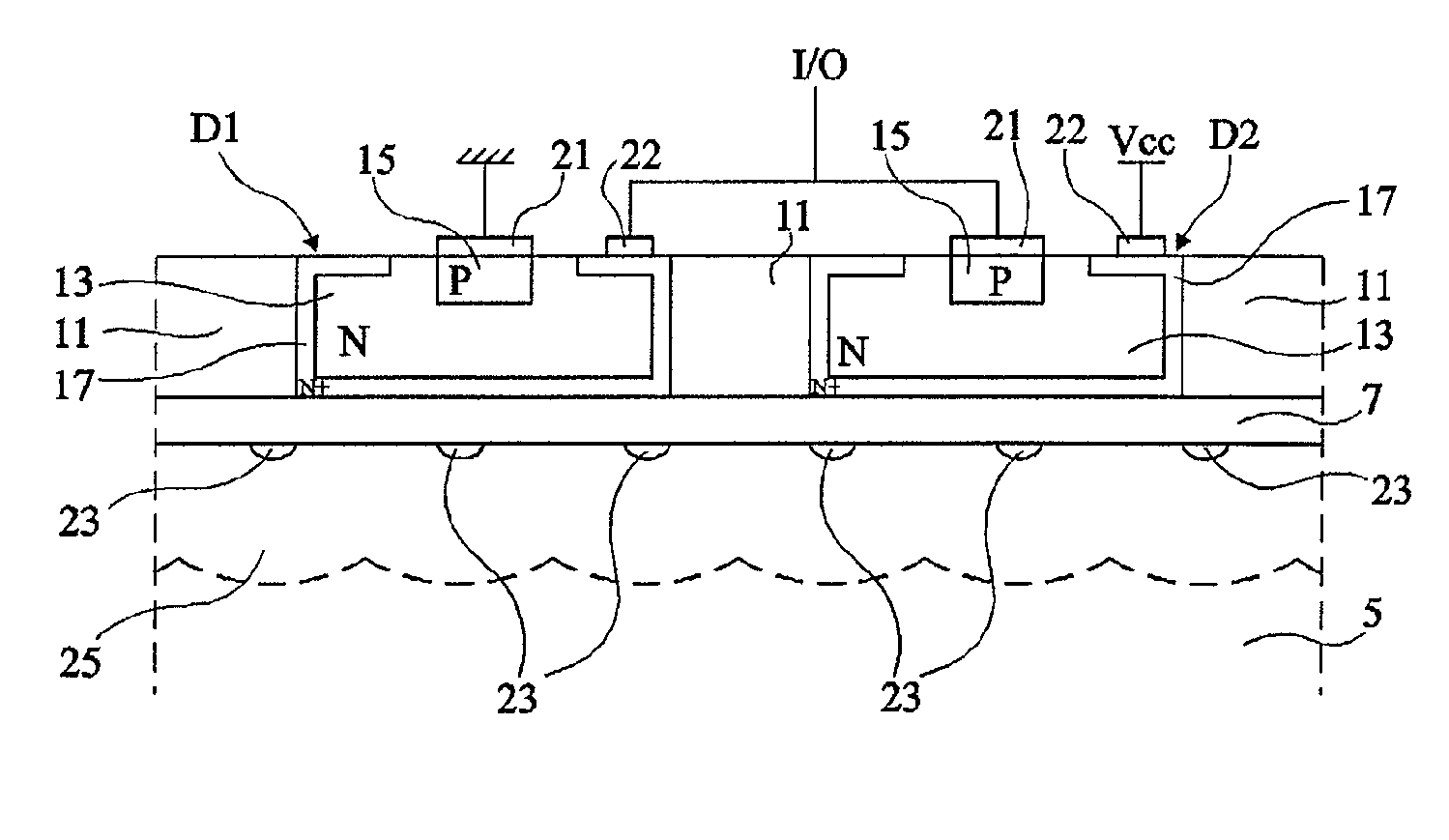
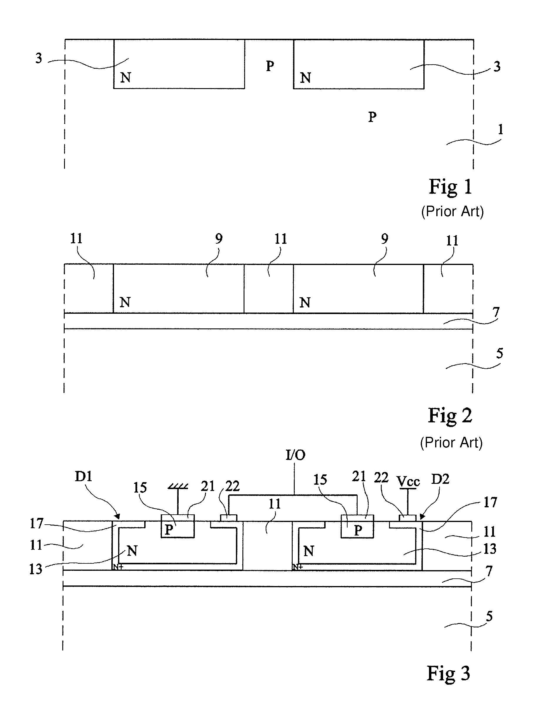
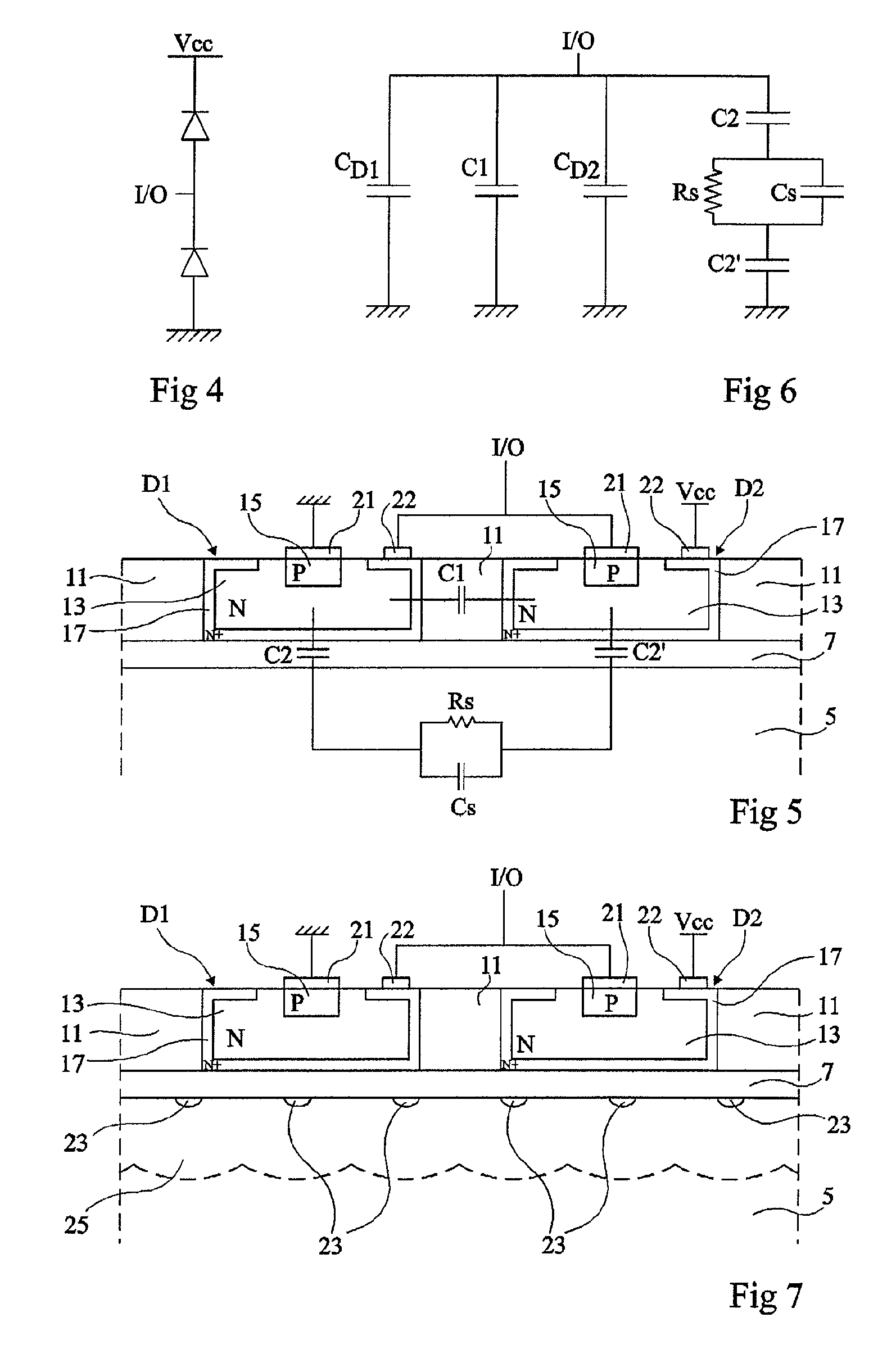
[0019]FIG. 3 shows two adjacent diodes D1 and D2 of protection against overvoltages. These diodes are placed side by side and are formed on an SOI-type structure comprising a thin semiconductor substrate formed on an insulating layer 7, itself formed on a semiconductor support 5. Diodes D1 and D2, which are identical, are laterally insulated by insulating regions 11, for example made of silicon oxide. Each diode comprises an N-type doped well 13 in which is formed a P-type doped region 15. The well is surrounded (bottom, lateral walls and part of its upper surface) with a heavily-doped N-type region 17. Anode and cathode contacts 21 and 22 are formed on region 15 and on region 17 in contact with well 13. Anode 21 of d...


PUM


Abstract

A structure including at least two neighboring components, capable of operating at high frequencies, formed in a thin silicon substrate extending on a silicon support and separated therefrom by an insulating layer, the components being laterally separated by insulating regions. The silicon support has, at least in the vicinity of its portion in contact with the insulating layer, a resistivity greater than or equal to 1,000 ohms.cm.

Description

BACKGROUND OF THE INVENTION[0001]1. Field of the Invention[0002]The present invention relates to a structure comprising high-frequency components, for example a protection structure.[0003]2. Discussion of the Related Art[0004]Generally, electronic components are formed either in a solid substrate semiconductor wafer, or in a semiconductor-on-insulator (SOI) layer.[0005]FIG. 1 shows the upper portion of a doped solid substrate 1 of a first conductivity type, for example, P, in which are formed several doped wells 3 of a second conductivity type, for example N. High-frequency electronic components can then be formed in wells 3. The isolation between wells 3 results from an appropriate biasing of the PN junctions between wells 3 and substrate 1. The capacitances between a well 3 and substrate 1 and between two neighboring wells 3 are often non-negligible as compared with the specific capacitances of the components formed in wells 3 and this is a problem, especially in the field of high...

Claims


Application Information

Patent Timeline
Patent Type & Authority Patents(United States)
IPC IPC(8): H01L29/72
CPCH01L21/76264H01L27/0251H01L27/0814H01L27/1203H01L29/06H01L29/8611
Inventor SIMONNET, JEAN-MICHELLHORTE, ANDREPOVEDA, PATRICK
Owner STMICROELECTRONICS SRL
Why Eureka
Try Eureka