Substrate, method for manufacturing substrate, and elastic wave device

a technology of substrate and acoustic wave, which is applied in the direction of printed circuit manufacturing, printed circuit aspects, final product manufacturing, etc., can solve the problems of increasing the size of an entire surface acoustic wave device, increasing the distance between the electrode lands, and reducing the bonding strength of each bump, so as to increase the thickness, increase the thickness, and increase the thickness

Active Publication Date: 2017-10-26
MURATA MFG CO LTD
View PDF0 Cites 0 Cited by
  • Summary
  • Abstract
  • Description
  • Claims
  • Application Information

AI Technical Summary

Benefits of technology

[0007]Preferred embodiments of the present invention provide substrates that enable stray capacitance between electrode lands to be decreased and that achieves decreases in size, methods for manufacturing the substrates, and elastic wave devices including the substrates.

Problems solved by technology

However, the increase in the distance between the electrode lands increases the size of an entire surface acoustic wave device.
There is, however, a possibility that the decrease in the area of each electrode land decreases a bonding strength that each bump provides.

Method used


Image

  • Substrate, method for manufacturing substrate, and elastic wave device
  • Substrate, method for manufacturing substrate, and elastic wave device
  • Substrate, method for manufacturing substrate, and elastic wave device

Examples


Embodiment Construction

[0031]Preferred embodiments of the present invention will hereinafter be described in detail with reference to the drawings to clarify the present invention.

[0032]The preferred embodiments are described by way of example in the present disclosure, and features thereof may be partially replaced or combined between different preferred embodiments.

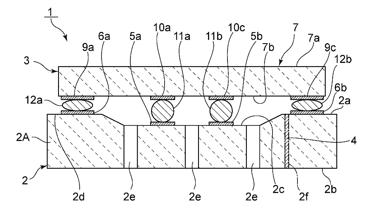
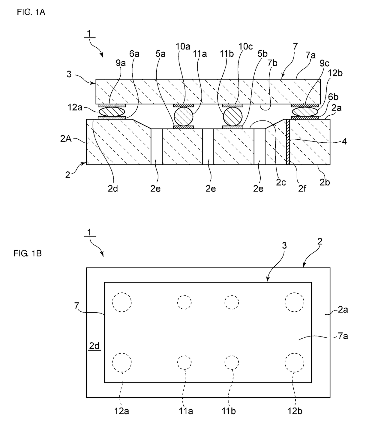
[0033]FIGS. 1A and 1B are a sectional front view and a plan view of a surface acoustic wave device according to a first preferred embodiment of the present invention. A surface acoustic wave device 1 includes a substrate 2 according to a preferred embodiment of the present invention. The substrate 2 includes a substrate main body 2A made of an insulating material. Ceramics, such as alumina, are preferably used as the insulating material. In the surface acoustic wave device 1, a surface acoustic wave element 3 is mounted above the substrate 2.

[0034]The substrate main body 2A includes a first main surface 2a and a second main surface 2b. The fi...


PUM


Abstract

A substrate includes a substrate main body that includes a first main surface and a second main surface facing the first main surface. First electrode lands are disposed inside a recessed portion of the first main surface of the substrate main body. Second electrode lands are disposed in a region outside the recessed portion. The first electrode land and the second electrode land are connected to different electric potentials.

Description

CROSS REFERENCE TO RELATED APPLICATIONS[0001]This application claims the benefit of priority to Japanese Patent Application No. 2015-006767 filed on Jan. 16, 2015 and is a Continuation Application of PCT Application No. PCT / JP2016 / 051005 filed on Jan. 14, 2016. The entire contents of each application are hereby incorporated herein by reference.BACKGROUND OF THE INVENTION1. Field of the Invention[0002]The present invention relates to a substrate including electrode lands on a main surface, a method for manufacturing the substrate, and an elastic wave device.2. Description of the Related Art[0003]Conventionally, junction structures between electronic component elements and packaging substrates with bumps are widely used. For example, according to Japanese Unexamined Patent Application Publication No. 2012-186633, electrode lands for signal-side terminals and electrode lands for ground terminals are disposed on a die-attachment surface of a packaging substrate. The electrode lands for ...

Claims


Application Information

Patent Timeline
Patent Type & Authority Applications(United States)
IPC IPC(8): H01L41/083H03H9/02H01L41/312H03H9/125H01L41/277
CPCH01L41/083H01L41/277H01L41/312H03H9/125H03H9/02559H03H9/02031H03H9/02574H03H9/059H05K1/0306H05K3/3436H05K2201/094Y02P70/50H10N30/50H10N30/057H10N30/072
Inventor KANEDA, AKIO
Owner MURATA MFG CO LTD
Why Eureka
Try Eureka