Common mode noise filter

Pending Publication Date: 2021-09-30
PANASONIC INTELLECTUAL PROPERTY MANAGEMENT CO LTD
View PDF0 Cites 0 Cited by
  • Summary
  • Abstract
  • Description
  • Claims
  • Application Information

AI Technical Summary

Benefits of technology

The present disclosure is about a common mode noise filter that reduces stray capacitance and prevents inconsistent differential signals in a high-frequency band. This is achieved by arranging the first pad, second pad, first spiral conductor, and second spiral conductor so that they don't overlap each other in top view. The technical effect of this is to enable the use of the common mode noise filter in a high-frequency band without increasing insertion loss.

Problems solved by technology

As a result, a significant stray capacitance is generated among pads 2a to 5a, which causes inconsistent differential signals in a high-frequency to increase insertion loss, posing a problem of difficulty in using the common mode noise filter in a high-frequency band.

Method used


Image

  • Common mode noise filter
  • Common mode noise filter
  • Common mode noise filter

Examples


Embodiment Construction

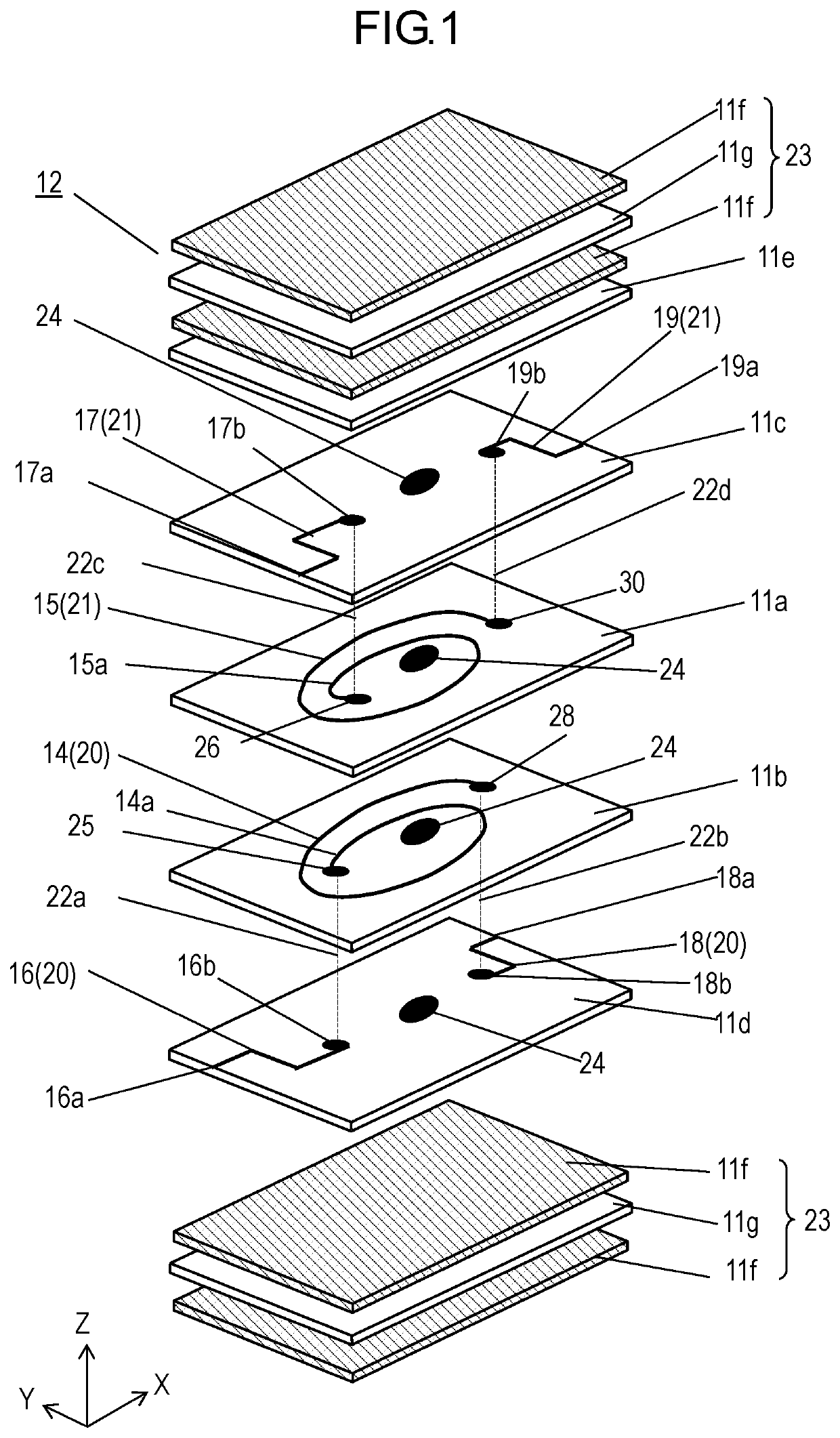
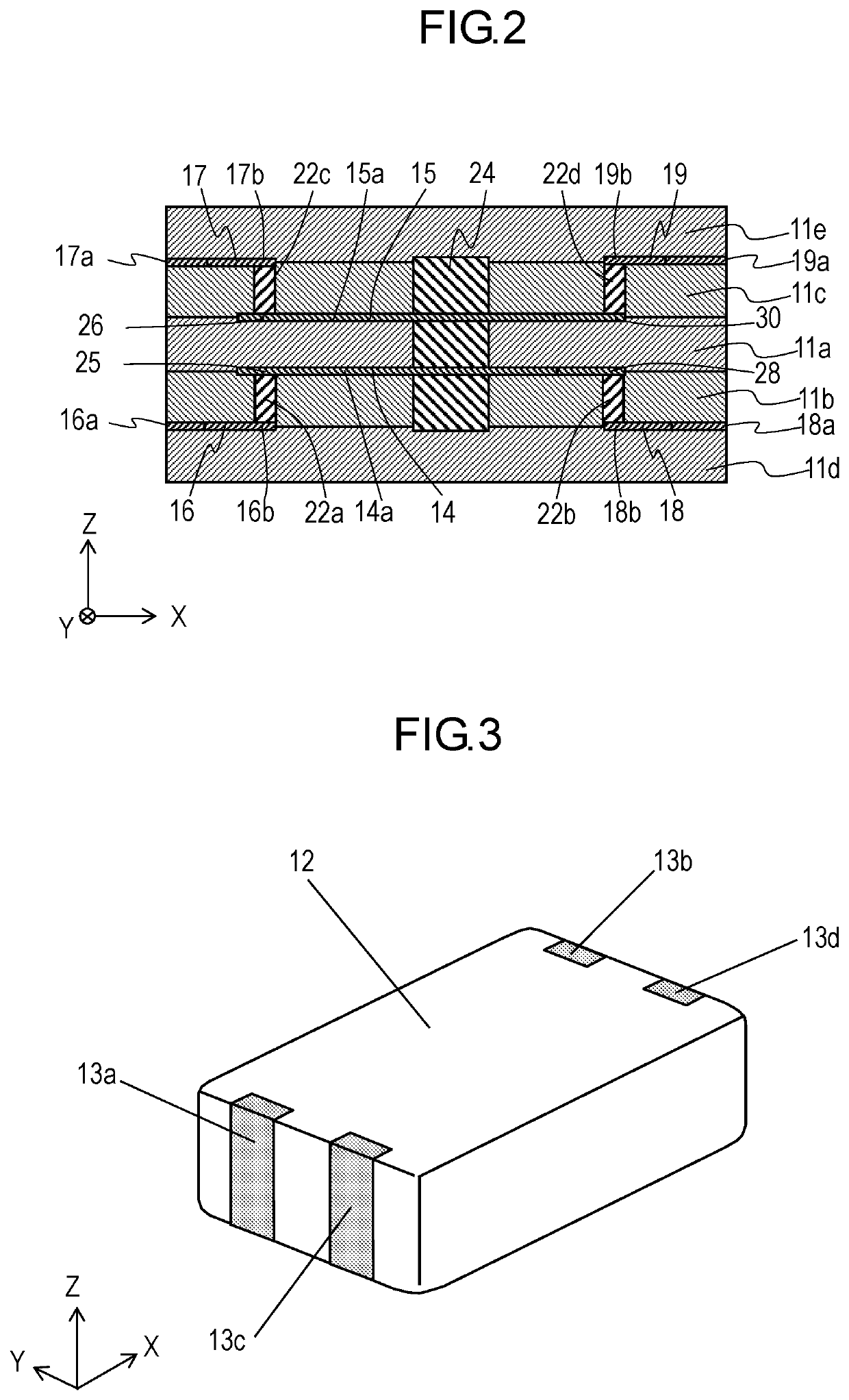
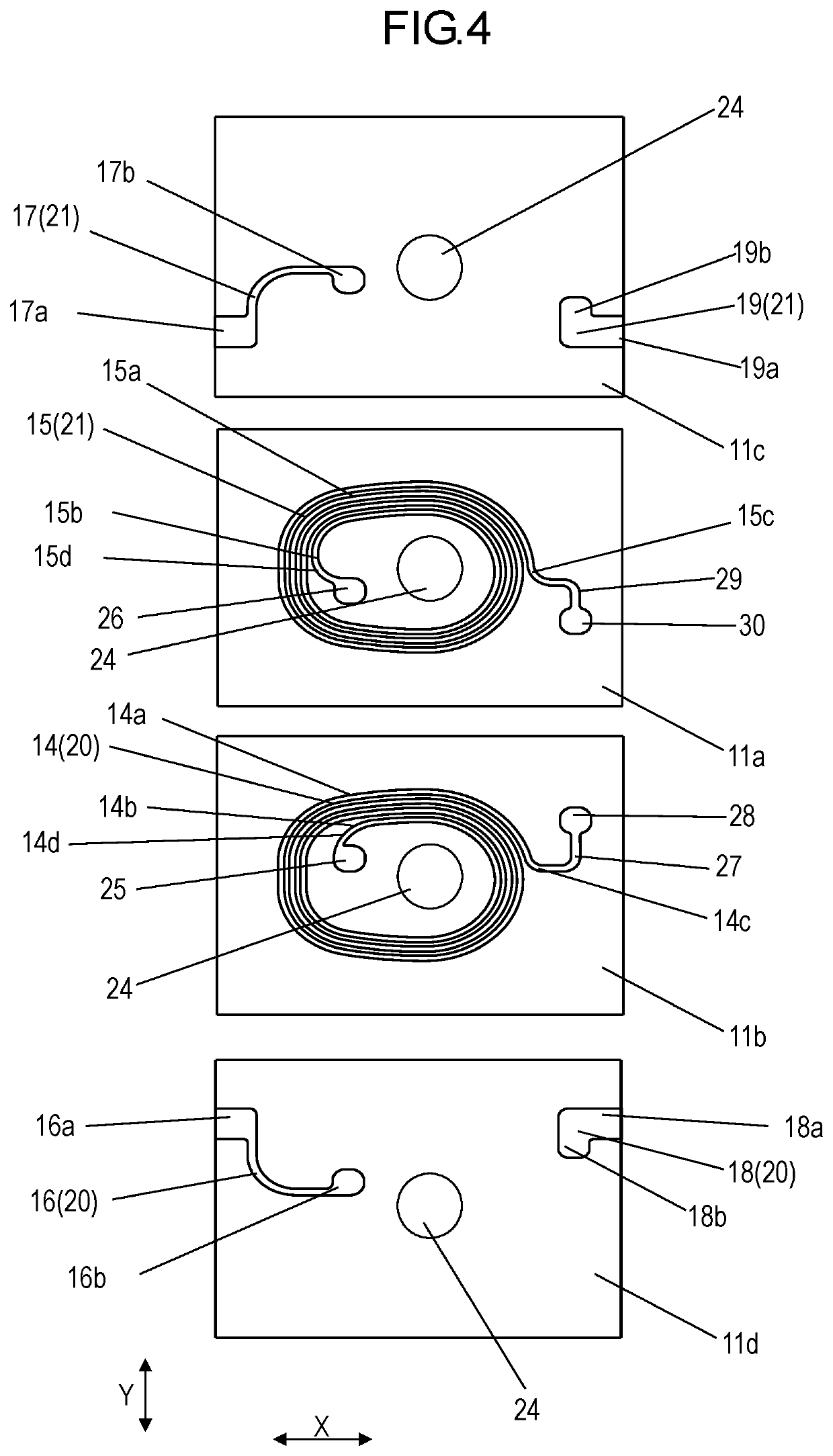
[0015]A common mode noise filter according to aspects of the present disclosure will now be described.

[0016]A common mode noise filter according to a first aspect includes a first insulator layer, a first conductor, and a second conductor. The first insulator layer includes a main surface and a back surface. The first conductor is disposed on the back surface of the first insulator layer. The second conductor is disposed on the main surface of the first insulator layer. The first conductor includes a first spiral body, a first pad, and a first connecting portion. The first spiral body is disposed at a position where at least part of the first spiral body overlaps the second conductor as viewed from a direction that the main surface of the first insulator layer faces. The first spiral body is in a spiral shape. The first pad is disposed inside the first spiral body on the back surface of the first insulator layer. The first connecting portion connects the first spiral body and the fi...


PUM


Abstract

An object of the present disclosure is to provide a common mode noise filter that can be used in a high-frequency band. The common mode noise filter of the present disclosure includes first to fifth insulator layers and stacked body in which first to fifth insulator layers are stacked along a vertical direction. The common mode noise filter further includes first spiral conductor and second spiral conductor that are formed inside stacked body and face each other across first insulator layer. The common mode noise filter further includes first pad connected to an inner end of first spiral conductor and second pad connected to an inner end of second spiral conductor. Neither first pad nor second pad overlaps each of first spiral conductor and second spiral conductor in top view.

Description

TECHNICAL FIELD[0001]The present disclosure relates to a common mode noise filter used for various electronic devices such as digital devices, audio visual (AV) devices, and information communication terminals.BACKGROUND ART[0002]As illustrated in FIG. 6, a conventional common mode noise filter of this type includes conductors 2 to 5 disposed on upper surfaces of insulating layers la to 1d, respectively. Pad 2a formed at one end of conductor 2 and pad 3a formed at one end of conductor 3 are connected through via electrode 6a to form coil 7. At the same time, pad 4a formed at one end of conductor 4 and pad 5a formed at one end of conductor 5 are connected through via electrode 6b to form coil 8. In addition, conductor 3 and conductor 4 are spirally wound, and the other end of each of conductors 2 to 5 is connected to an external electrode (not illustrated; the same applies to the following).[0003]Examples of known technical documents related to the present disclosure include PTL 1.CI...

Claims


Application Information

Patent Timeline
IPC IPC(8): H01F17/00H01F27/28H01F27/29H01F17/04H03H7/09H03H7/42
CPCH01F17/0013H01F27/2804H01F27/292H01F17/04H01F2027/2809H03H7/427H01F2017/0073H01F2017/0093H03H7/09H01F27/29H01F2017/0066H01F17/0033H03H2001/0085
Inventor KAWASHIMA, TAKUJINAWATE, MASAKATSUONODERA, YUTANAKA, HIDEKI
Owner PANASONIC INTELLECTUAL PROPERTY MANAGEMENT CO LTD
Why Eureka
Try Eureka