Optical coupling arrangement having low coupling loss and high production yield

a coupling arrangement and low coupling loss technology, applied in the field of optical coupling arrangements, can solve the problems of reducing the insertion loss of these devices, increasing the fraction of devices fabricated which must be discarded due to defects, and reducing the size of these structural features, so as to reduce the effective width of the gap, reduce the effective width, and reduce the effect of tapering

Inactive Publication Date: 2005-05-10
YU GUOMIN
View PDF9 Cites 51 Cited by
  • Summary
  • Abstract
  • Description
  • Claims
  • Application Information

AI Technical Summary

Benefits of technology

[0011]An optical coupling arrangement has a first transition region having a plurality of first segmented waveguides and a plurality of transverse segments, of alternating indices of refraction, at least some of which traverse the first segmented waveguides. The first transition region is delimited by the transverse segments. In some embodiments of the invention a second transition region having a plurality of second segmented waveguides is arranged adjacent the first transition region with each one of the second segmented waveguides of the second transition region being aligned with a respective one of the first segmented waveguides of the first transition region. The transverse segments provide mode expansion in respect to a direction from the first transition region to the second transition region whereas individual ones of the first and second segmented waveguides provide mode contraction in respect to the same direction. The mode contraction results in effective tapering of the first and second segmented waveguides which, in turn, provides a reduced effective width of a gap between adjacent ones of the first segmented waveguides. The reduced effective width is used to lower the coupling loss of the optical coupling arrangement. This is achieved in combination with the mode expansion provided by the transverse segments which allows optical power from an optical signal input into the arrangement to gradually couple into the first segmented waveguides. The optical coupling arrangement is used in optical coupling devices for combining / splitting optical signals and to provide a reduced insertion loss of these devices. The reduction in the insertion loss allows the optical couplers to be fabricated with dimensions large enough for production with a high production yield. The optical coupling devices are also used in other devices such as Mach-Zehnder interferometers and arrayed waveguide grating demultiplxers / multiplexers.

Problems solved by technology

These optical waveguide devices typically have a planar waveguide structure and the insertion loss of these devices decreases with decreasing size of some of the structural features of the structure.
However, during production the fraction of devices fabricated which must be discarded due to defects increases with decreasing size of these structural features.
The insertion loss is therefore decreased at the expense of a lower production yield.
As such, there is a minimum size for these features for which a reasonable production yield is achieved but at this minimum size the insertion loss is still too high.
There are gaps between adjacent ones of the M waveguides of the first array at a junction between the slab waveguide and the first array and these gaps result in a mismatch between the optical field of any one of the N optical signals in the slab waveguide and the optical fields of corresponding M optical signals in the M waveguides of the first array.
This mismatch results in a coupling loss which contributes to a major portion of the star coupler's insertion loss.
However, the minimum width of the gaps for which these star coupler's can be fabricated with an acceptable production yield is still too large to produce a low insertion loss.
Furthermore, with conventional technology for fabricating planar waveguide structures, a low production yield is obtained when star couplers are fabricated with such a small width of the gaps.
Some advances have been made to improve the performance of these devices; however, further advances are still limited by the processes used to fabricate these devices.
However, such a coupling loss is still too high.
Furthermore, for a width Wg=2 μm, a significant portion of wafers on which star couplers are produced are unusable due to fabrication defects and this results in low production yield.

Method used


Image

  • Optical coupling arrangement having low coupling loss and high production yield
  • Optical coupling arrangement having low coupling loss and high production yield
  • Optical coupling arrangement having low coupling loss and high production yield

Examples


Embodiment Construction

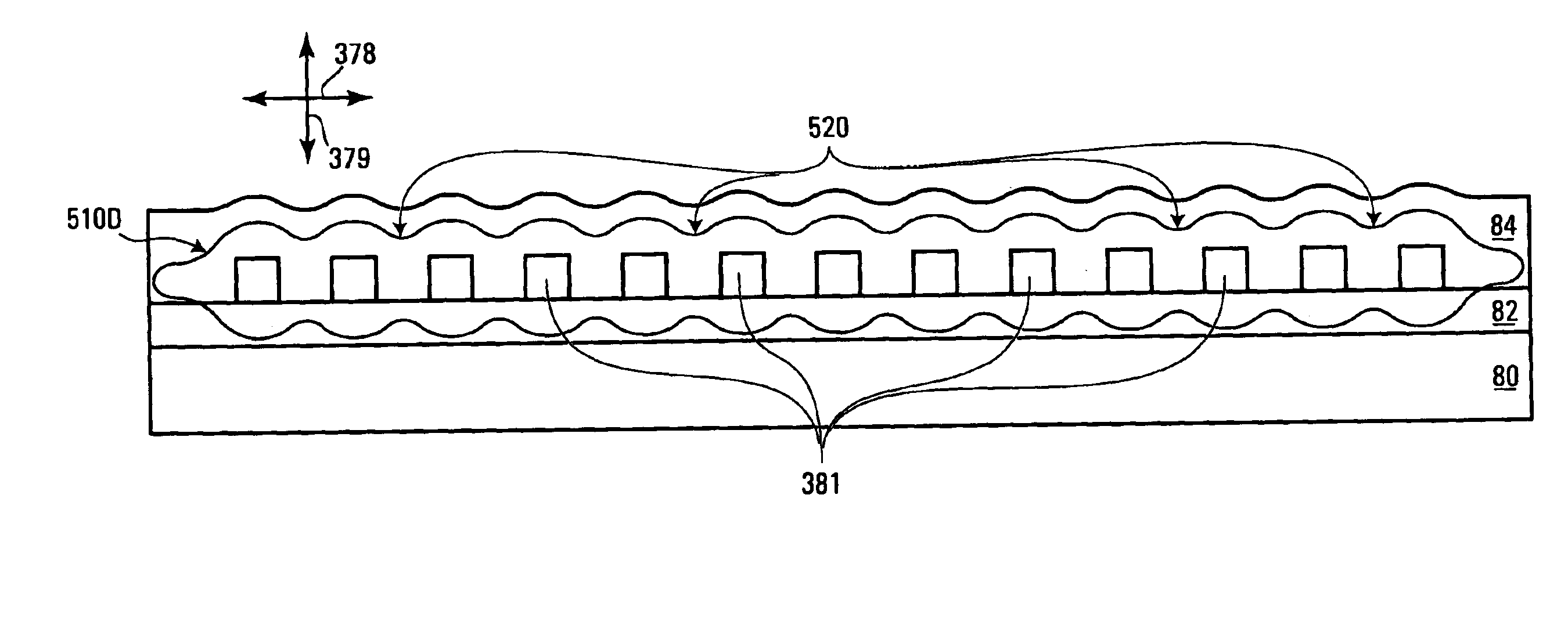
[0038]Referring to FIG. 3A shown is a top view of an example star coupler according to one embodiment of the invention. The star coupler is generally indicated by 301 and has a first coupling waveguide, shown as slab waveguide 310, with preferably circularly curved ends 315a and 315b. In FIG. 3C, a cross-sectional view of the optical coupler 301 through the slab waveguide 310 shows a core 311 of the slab waveguide 310 located between layers 82 and 84 of under-cladding and top-cladding, respectively. Referring back to FIG. 3A, there is a first array 314 of first waveguides 326 and a second array 312 of second waveguides 324 at curved end 315a. A first transition region 332 has first and second ends 357 and 358, respectively, and is adjacent the slab waveguide 310. A second transition region 322 is located between the first transition region 332 and the first array 314.

[0039]The first transition region 332 has a plurality of first transverse segments 360 of a core material, and a plur...


PUM


Abstract

An optical coupling arrangement has a first transition region having a plurality of first segmented waveguides and a plurality of transverse segments of alternating indices of refraction with at least some of the transverse segments traversing the first segmented waveguides. The first segmented waveguides are formed by core segments in some of the transverse segments. The arrangement may also have a second transition region having a plurality of second segmented waveguides each aligned with a respective one of the first segmented waveguides. The arrangement is manufactured with a high production yield and is used in an optical coupling device for combining / splitting optical signals to reduce the insertion loss. The optical coupling device is also used in other devices such as Mach-Zehnder devices and arrayed waveguide grating demultiplexers / multiplexers.

Description

FIELD OF THE INVENTION[0001]This invention relates to optical coupling arrangements for optical couplers and other optical devices using these optical couplers. In particular, the invention relates to improving the insertion loss of the optical couplers while maintaining a high production yield during manufacturing.BACKGROUND OF THE INVENTION[0002]DWDM (Densed Wavelength Division Multiplexing) systems need optical waveguide devices such as star couplers, branch power splitters, AWG (Arrayed Waveguide Grating) multiplexers / demultiplexers and VOA (Variable Optical Attenuators) to control, combine and separate optical signals having different wavelengths. These optical waveguide devices typically have a planar waveguide structure and the insertion loss of these devices decreases with decreasing size of some of the structural features of the structure. However, during production the fraction of devices fabricated which must be discarded due to defects increases with decreasing size of t...

Claims


Application Information

Patent Timeline
Patent Type & Authority Patents(United States)
IPC IPC(8): G02B6/28G02B6/34
CPCG02B6/2808G02B6/12011
Inventor YU, GUOMIN
Owner YU GUOMIN
Why Eureka
Try Eureka