Manufacturing method for optical fiber array for optical coupling and coupling method and device

A fiber array and optical coupling technology, which is applied in the field of communication and can solve problems such as the difficulty of coupling between chips and fibers

Active Publication Date: 2016-06-29
GUANGXUN SCI & TECH WUHAN
View PDF7 Cites 18 Cited by
  • Summary
  • Abstract
  • Description
  • Claims
  • Application Information

AI Technical Summary

Problems solved by technology

The thickness of a silicon photonics chip is generally on the order of hundreds of microns, and the etching depth of the SSC coupling end is usually smaller than the thickness of the chip. Beca

Method used


Image

  • Manufacturing method for optical fiber array for optical coupling and coupling method and device
  • Manufacturing method for optical fiber array for optical coupling and coupling method and device
  • Manufacturing method for optical fiber array for optical coupling and coupling method and device

Examples


Embodiment Construction

[0039] The coupling method of the optical fiber array and the silicon optical chip in the invention will be described in detail below with reference to the embodiments and the accompanying drawings.

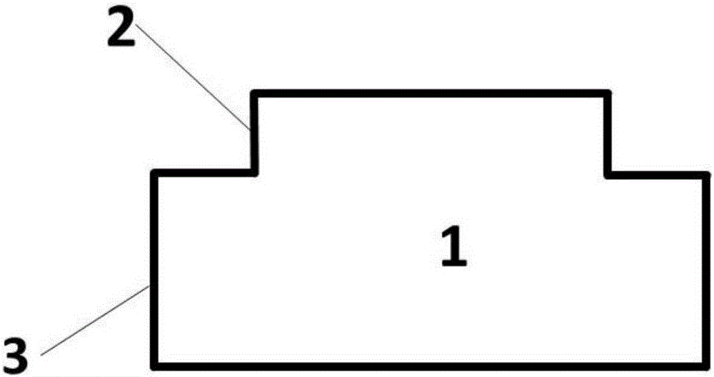
[0040] figure 1 It is a schematic diagram of the silicon photonics chip 1 to be coupled. The chip coupling end face 2 is a coupling end face with a specific coupling structure, which is etched by an inductively coupled plasma process in a CMOS process. The chip dicing end face 3 is a dicing end face. In order to avoid damaging the coupling end face during dicing, a protective distance is generally reserved between the chip coupling end face and the dicing end face during chip processing, so a stepped chip end face is formed.

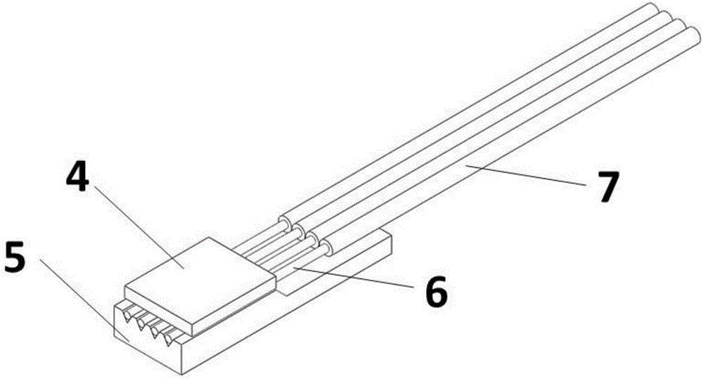
[0041] figure 2 is directed at figure 1 Assembly of fiber arrays fabricated at the chip scale. It consists of a 4-core optical fiber array 6 with the coating layer 7 removed at the end, a V-groove 5, and a cover glass 4 fixed by dispensing glue. The thi...


PUM


Abstract

The invention provides a manufacturing method for an optical fiber array for optical coupling and a coupling method and device.The manufacturing method for the optical fiber array comprises the following steps that naked fibers of the optical fiber array are pressed into a V-shaped groove, the tail end of a bare wire is aligned to the tail end of the V-shaped groove, the bare wire pressed into the V-shaped groove is covered with cover glass to be fixed, the cover glass does not cover the tail end of the V-shaped groove, the distance between the tail end of the cover glass and the tail end of the V-shaped groove is larger than the depth distance between steps of a silicon optical chip coupled to the optical fiber array, and the tail end of the optical fiber array is supported under the V-shaped groove to form one step; an adhesive is dispensed on the portion, not covered with the cover glass, of the bare wire so as to fix the bare wire; a filler aligned to the tail end of the V-shaped groove is applied to the step at the tail end of the optical fiber array; the end face of the optical fiber array is polished, the filler is removed after polishing is performed, and the step is exposed.By adopting the step-type optical fiber array, the problem that coupling losses are large due to the fact that a common optical fiber array is far away from the coupling end face of the chip is solved.

Description

technical field [0001] The present invention relates to a method for manufacturing an optical communication device, in particular to a method for manufacturing an optical fiber array for optical coupling, in particular to a method for manufacturing an optical fiber array applied to silicon optical chip coupling and its coupling method, silicon optical chip Device, the invention belongs to the communication field. Background technique [0002] In recent years, with the continuous development of CMOS technology, the feature size of IC chip tape-out process has become smaller and smaller, which provides a broad development space for silicon photonics based on submicron-sized optical waveguides. Compared with traditional InP integrated optoelectronic chips, silicon photonics has many advantages such as small size, high integration, and low cost. As one of the most promising solutions for on-chip optical interconnection, silicon photonics has become a hot topic in the industry. ...

Claims


Application Information

Patent Timeline
IPC IPC(8): G02B6/26
CPCG02B6/26
Inventor 黄钊张博胡毅马卫东
Owner GUANGXUN SCI & TECH WUHAN
Why Eureka
Try Eureka