System and tapered waveguide for improving light coupling efficiency between optical fibers and integrated planar waveguides and method of manufacturing same

A waveguide light and tapered wave technology, applied in the field of optical mode converters, can solve the problems of not providing high coupling efficiency, wavelength independence, reliability, manufacturability, durability, and robustness, and achieve increased optical Effect of Coupling Efficiency

Inactive Publication Date: 2007-02-28
克咯拉姆达技术有限公司
View PDF0 Cites 21 Cited by
  • Summary
  • Abstract
  • Description
  • Claims
  • Application Information

AI Technical Summary

Problems solved by technology

Unfortunately, these technologies do not provide the combination of high coupling efficiency, wavelength independence, reliab

Method used


Image

  • System and tapered waveguide for improving light coupling efficiency between optical fibers and integrated planar waveguides and method of manufacturing same
  • System and tapered waveguide for improving light coupling efficiency between optical fibers and integrated planar waveguides and method of manufacturing same
  • System and tapered waveguide for improving light coupling efficiency between optical fibers and integrated planar waveguides and method of manufacturing same

Examples


Embodiment Construction

[0019] The following detailed description, which refers to and considers in conjunction with the accompanying drawings, describes and illustrates one or more specific embodiments of the present invention. These embodiments are provided not to be limiting but to exemplify and teach the invention, shown and described in sufficient detail to enable those skilled in the art to practice the invention. Thus, where appropriate to avoid obscuring the invention, the description may omit certain information known to those skilled in the art.

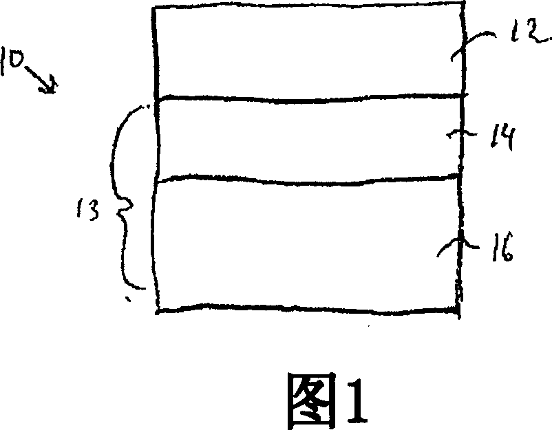
[0020] Turning now to the drawings, and specifically to FIG. 1 , there is shown a schematic cross-sectional view of an exemplary starting material structure 10 for fabricating a tapered planar waveguide. A preferred starting material 10 for fabricating 1-D and 2-D waveguides is a silicon-on-insulator (SOI) structure. The SOI starting material 10 comprises a layer 12 of crystalline silicon grown on a planar substrate structure 13 . The planar sub...


PUM


Abstract

A tapered waveguide optical mode transformer (20) includes a tapered core formed on a planar substrate structure (16). To vertically taper the core (21), steps (22) are etched into the top surface of the core. The steps have depths and lengths along the optical axis of tapered waveguide that are selected to transform the optical mode characteristics of a desired optical fiber to the optical mode characteristics of a desired planar waveguide. The core can also be tapered horizontally to form a 2-D tapered waveguide. The tapered waveguide can be integrally included in planar lightwave circuits (PLCs) to reduce light coupling losses between optical fibers and the PLC waveguides.

Description

technical field [0001] The present invention relates generally to planar lightwave circuits and, more particularly, to optical mode converters for efficiently coupling optical fibers to planar integrated waveguides. Background technique [0002] Planar lightwave circuits (PLCs) send and receive signals both for short-range data and for long-distance telecommunications systems. For optimal operation, PLCs have functional optics such as waveguides. These waveguides should be sufficiently small in size that dense integration of waveguide optics including sharp bends in the waveguides is possible on a single chip. [0003] High index contrast material systems are well suited for fabricating PLCs. Such a material system can be formed on a silicon-on-insulator (SOI) substrate as a core layer of silicon with a refractive index of about 3.5, surrounded on both sides by cladding layers of quartz with a refractive index of about 1.5. A waveguide formed in such a structure is called...

Claims


Application Information

Patent Timeline
IPC IPC(8): G02B6/122G02B6/136G02B6/30
CPCG02B6/305G02B6/1228G02B6/136G02B2006/12195G02B6/14G02B6/12
Inventor 马苏·乔杜里托马斯·R·斯坦奇克迪安·理查森阿里耶勒·东瓦尔拉姆·奥龙摩西·奥龙
Owner 克咯拉姆达技术有限公司
Why Eureka
Try Eureka