Waveguide coupling structure and light emitter system

A technology of coupling structure and conductive structure, applied in the field of optical communication, can solve the problems of difficulty, violation of the integrated development of optical devices, low optical coupling efficiency of lasers and silicon optical chips, etc., achieve low optical signal loss and improve optical coupling efficiency , to ensure the effect of structure miniaturization

Active Publication Date: 2020-06-05
BEIJING UNIV OF POSTS & TELECOMM
View PDF15 Cites 3 Cited by
  • Summary
  • Abstract
  • Description
  • Claims
  • Application Information

AI Technical Summary

Problems solved by technology

Based on this, the existing technology uses a lens coupling system to improve the coupling efficiency, that is, a lens coupling system is inserted between the light source and the silicon photonic chip to transform the light beam emitted by the light source. It is necessary to couple and package the optical path between the optical input port, multiple lens groups, wavelength division multiplexing devices and detectors included in the lens coupling system. It can be seen that the optical path coupling of the above-mentioned multiple devices is a very difficult task. task, which in turn leads to low optical coupling efficiency of lasers and silicon photonic chips, and also violates the goal of miniaturization and integration of optical devices

Method used


Image

  • Waveguide coupling structure and light emitter system
  • Waveguide coupling structure and light emitter system
  • Waveguide coupling structure and light emitter system

Examples


Embodiment Construction

[0042] The following will clearly and completely describe the technical solutions in the embodiments of the present invention with reference to the accompanying drawings in the embodiments of the present invention. Obviously, the described embodiments are only some, not all, embodiments of the present invention. Based on the embodiments of the present invention, all other embodiments obtained by persons of ordinary skill in the art without making creative efforts belong to the protection scope of the present invention.

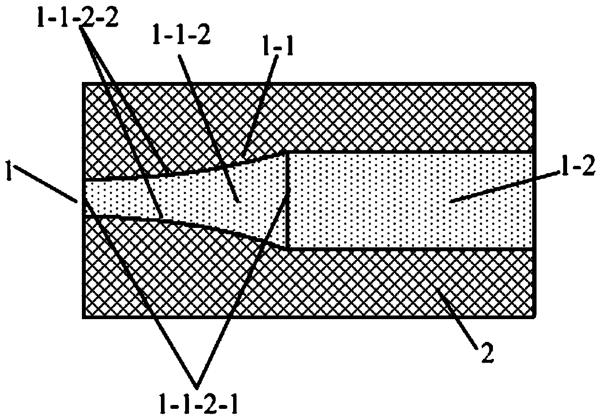
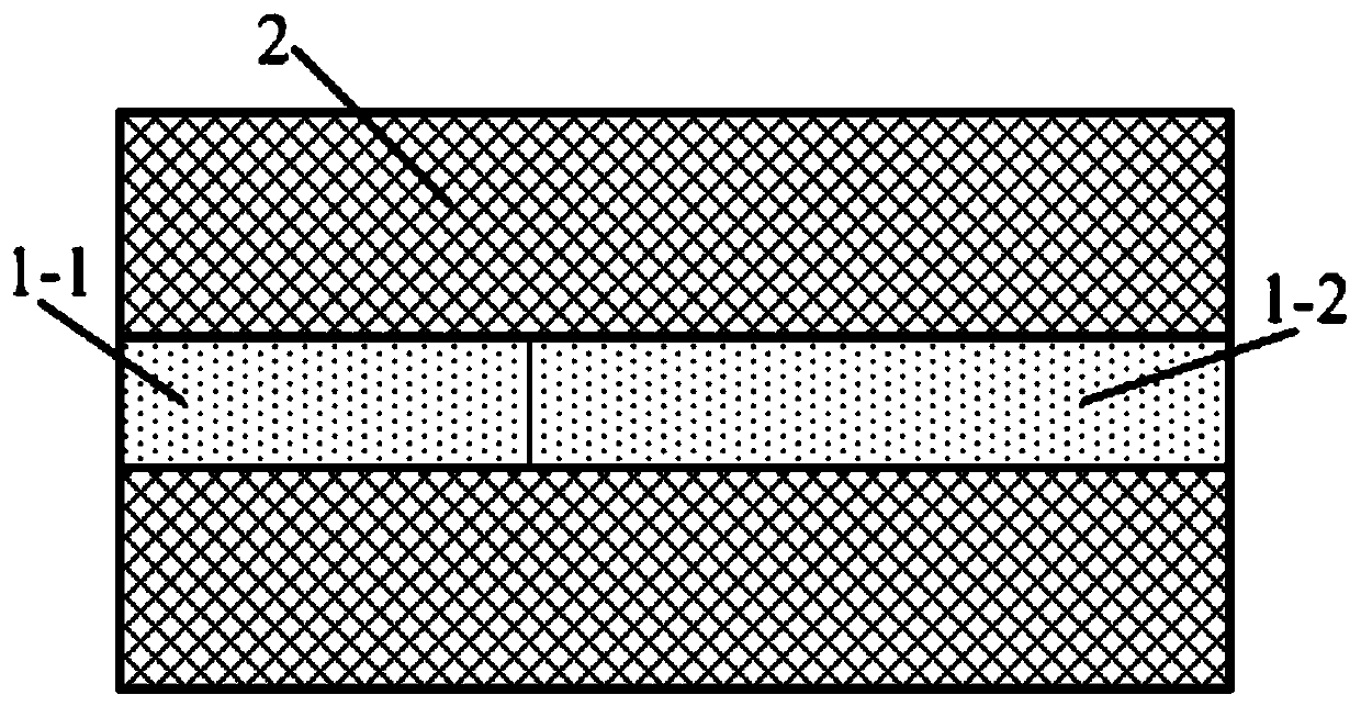
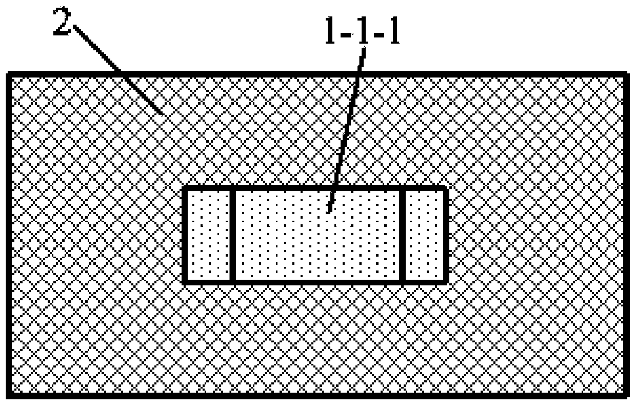
[0043] see Figure 1a~1c , Figure 1a~1cIt is a schematic diagram of the three-view cross-sectional structure of the first waveguide coupling structure 8 provided by the embodiment of the present invention. The waveguide coupling structure includes: a waveguide core structure 1 and a first package with a refractive index lower than that of the waveguide core structure 1. Layer 2;

[0044] Wherein, the above-mentioned waveguide core structure 1 includes: a co...


PUM

PropertyMeasurementUnit
refractive indexaaaaaaaaaa

Abstract

The embodiment of the invention provides a waveguide coupling structure and a light emitter system. The waveguide coupling structure comprises a waveguide core structure and a first cladding, and thefirst longitudinal sectional area of the rectangular surface of the coupling structure of the waveguide core structure changes from small to large in the length direction of the coupling structure; the cross section of the coupling structure is a quadrangle of which the first opposite sides are parallel and the second opposite sides in curve change are symmetrical along the perpendicular bisectorof the cross section; one end surface of the conduction structure is coplanar with the connection surface of the coupling structure, the waveguide core structure is embedded in the first cladding, thesmall end surface of the coupling structure is coplanar with one end surface of the first cladding, and the other end surface of the conduction structure is coplanar with the other end surface of thefirst cladding. Therefore, by applying the technical scheme provided by the embodiment of the invention, the optical coupling efficiency can be improved on the basis of ensuring the miniaturization and integration of the structure.

Description

technical field [0001] The invention relates to the technical field of optical communication, in particular to a waveguide coupling structure and an optical transmitter system. Background technique [0002] Planar optical waveguide technology is a technology in which an optical waveguide is fabricated in a planar substrate and optical signals are transmitted in the waveguide. Devices produced using planar optical waveguide technology have the advantages of small size, low loss, high integration, and easy scale production. Therefore, planar optical waveguide technology is widely used in optical communication systems. How to use silicon photonics integration technology to develop high-speed optical modules with high bandwidth, low cost and high integration has become an urgent need. [0003] At present, passive silicon optical devices such as high-speed silicon optical modulators, high-speed detectors, low-loss transmission waveguides, and wavelength division multiplexing hav...

Claims


Application Information

Patent Timeline
Patent Type & Authority Applications(China)
IPC IPC(8): G02B6/12G02B6/42
CPCG02B6/12004G02B6/4202
Inventor 陈远祥付佳韩颖黄雍涛李凯乐余建国
Owner BEIJING UNIV OF POSTS & TELECOMM
Why Eureka
Try Eureka