Grating coupler with adjustable refractive index and manufacturing method thereof

A technology of grating coupler and manufacturing method, which is applied in the direction of fiber mechanical structure, etc., and can solve problems such as mode mismatch

Active Publication Date: 2014-07-02
BEIJING UNIV OF TECH
View PDF2 Cites 23 Cited by
  • Summary
  • Abstract
  • Description
  • Claims
  • Application Information

AI Technical Summary

Problems solved by technology

[0008] In order to solve the problem of mode mismatch between the output mode field of the ordinary uniform grating coupler and the mode field of the single-mode fiber existing in the prior art, the object of the present invention i

Method used


Image

  • Grating coupler with adjustable refractive index and manufacturing method thereof
  • Grating coupler with adjustable refractive index and manufacturing method thereof
  • Grating coupler with adjustable refractive index and manufacturing method thereof

Examples


Embodiment Construction

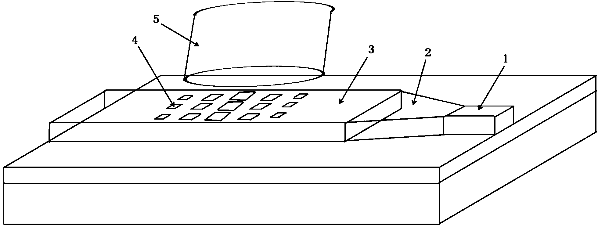
[0055] The structure and features of the present invention will be further described in detail below in conjunction with the drawings and embodiments. Such as figure 1 , figure 2 As shown, taking the SOI material as an example, a grating coupler with adjustable refractive index includes:

[0056] A substrate silicon layer 8;

[0057] A lower confinement layer 6 of a silicon waveguide, the confinement layer 6 is silicon dioxide material;

[0058] A silicon waveguide core layer 7, the waveguide core layer 7 is made under the upper confinement layer 6; the waveguide core layer 7 includes: the core layer of the submicron waveguide 1, the tapered waveguide 2 and the strip waveguide 3; the submicron waveguide 1 is a cuboid; the narrow end of the tapered waveguide 2 is connected to the submicron waveguide 1, and the other end is connected to the strip waveguide 3; the width of the tapered waveguide 2 is between the submicron waveguide 1 and the strip waveguide 3, for Reduce the ...


PUM


Abstract

The invention relates to the technical field of photonic devices, in particular to a method for manufacturing a grating coupler with an adjustable refractive index. The method is characterized in that a grating groove is of a sub-wavelength structure with different transverse duty ratios, and a grating has different duty ratios fy in the transverse direction, namely, the direction y, at different positions x in the longitudinal direction, namely, the direction x; the value of the duty ratio fx of the grating in the longitudinal direction is a fixed value between zero and one; the transverse duty ratio fy of the sub-wavelength structure forming the grating grooves at different positions x in the longitudinal direction is determined by leakage factor distribution alpha (x) needed by output Guassian field distribution G (x). The grating coupler of the structure can effectively reduce coupling losses in the optical fiber and waveguide coupling process.

Description

technical field [0001] The invention relates to the fields of optical communication and optical interconnection, in particular to the design and preparation of an optical waveguide coupling structure with adjustable refractive index. The grating coupler with this structure can effectively reduce the coupling loss when optical fiber and waveguide are coupled. Background technique [0002] Driven by low cost and low power consumption, silicon photonics technology is based on the SOI (silicon-on-insulator) platform. So far, a variety of silicon photonic devices have been prepared and photonic integration has been realized. Silicon photonics technology is considered to be the solution to the current integration problems. The most promising technique for power consumption and bandwidth issues in circuits. An important challenge facing silicon photonics technology at present is how to introduce laser light sources into and out of the photonic integrated circuit. Due to its high c...

Claims


Application Information

Patent Timeline
IPC IPC(8): G02B6/44
Inventor 郭霞武华韩明夫
Owner BEIJING UNIV OF TECH
Why Eureka
Try Eureka