Parallel optical interconnection module and method for manufacturing the same

a technology of optical interconnection and optical transmit/receive module, which is applied in the direction of optical elements, optical waveguide light guides, instruments, etc., can solve the problems of skew, emi (electromagnetic), affecting the operation efficiency of the system, and affecting the integration of the system, so as to minimize the coupling loss and increase the optical output

Inactive Publication Date: 2005-06-28
ELECTRONICS & TELECOMM RES INST
View PDF16 Cites 24 Cited by
  • Summary
  • Abstract
  • Description
  • Claims
  • Application Information

AI Technical Summary

Benefits of technology

[0010]The present invention is contrived to solve the above problems and an object of the present invention is to provide a parallel optical interconnection module capable of minimizing the coupling loss in the process in which an optical signal is transmitted and thus increasing the optical output.

Problems solved by technology

However, as information becomes large-scaled and the transfer speed becomes rapid in a next-generation information communication system consisting of a large-capacity parallel computer, an ATM switching system of over 1 Tb / s, and the like, electrical problems such as skew, EMI (electromagnetic interference), etc, are caused if this metal cable is employed.
Due to this, the operation efficiency of the system is lowered and the integration of the system is made difficult.
However, a large coupling loss is generated even though a slight alignment error is caused when the optical transmit / receive device and the optical fiber are coupled if the above optical interconnection technology is employed in the future in order to manufacture a parallel optical interconnect optical transmit / receive module having an extended function.

Method used


Image

  • Parallel optical interconnection module and method for manufacturing the same
  • Parallel optical interconnection module and method for manufacturing the same
  • Parallel optical interconnection module and method for manufacturing the same

Examples


Embodiment Construction

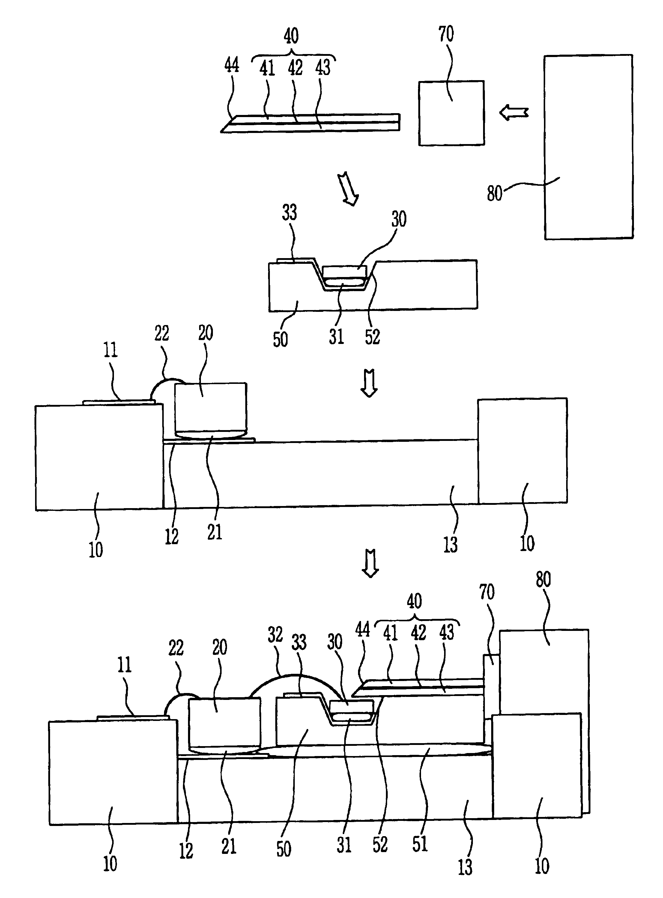
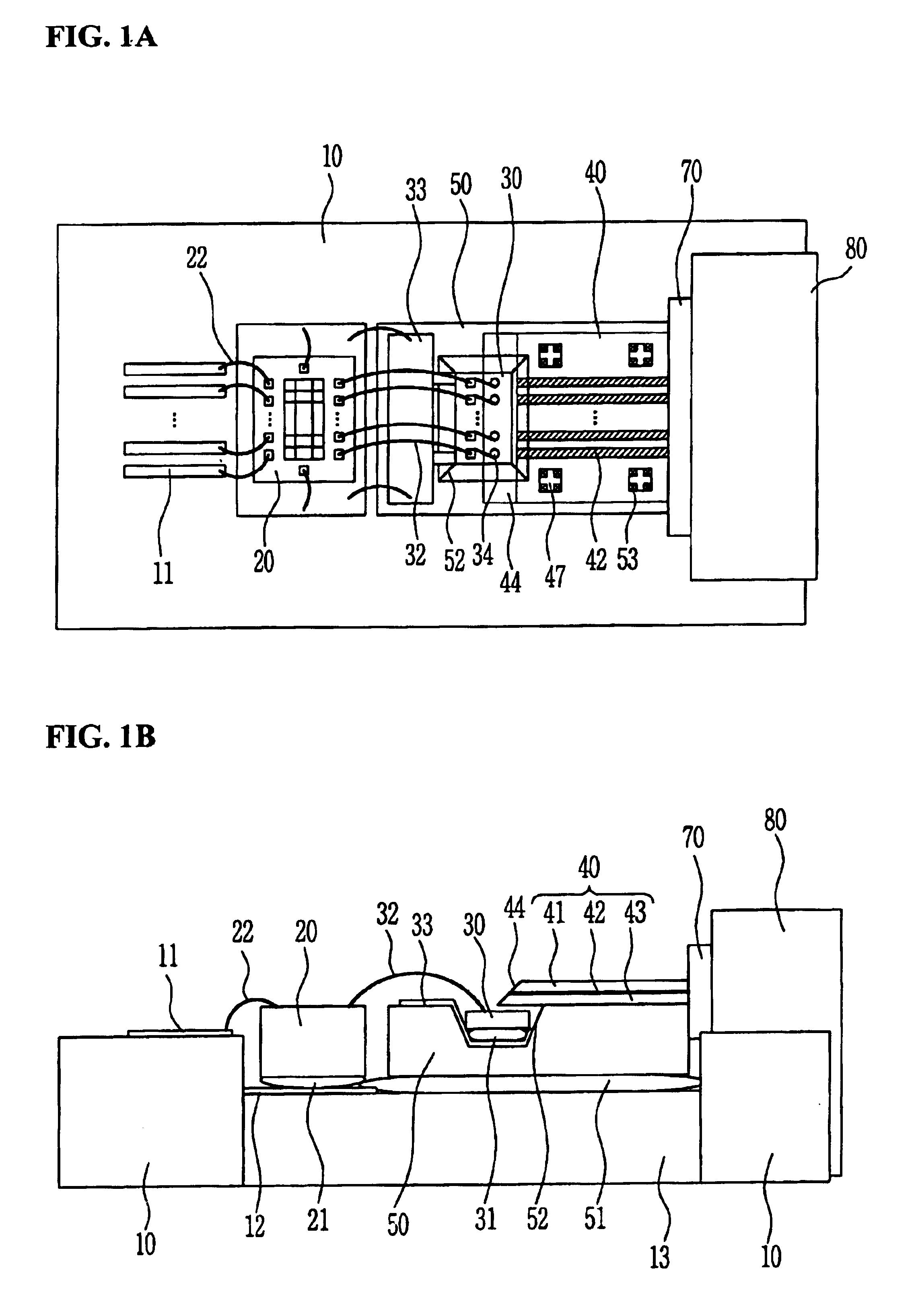
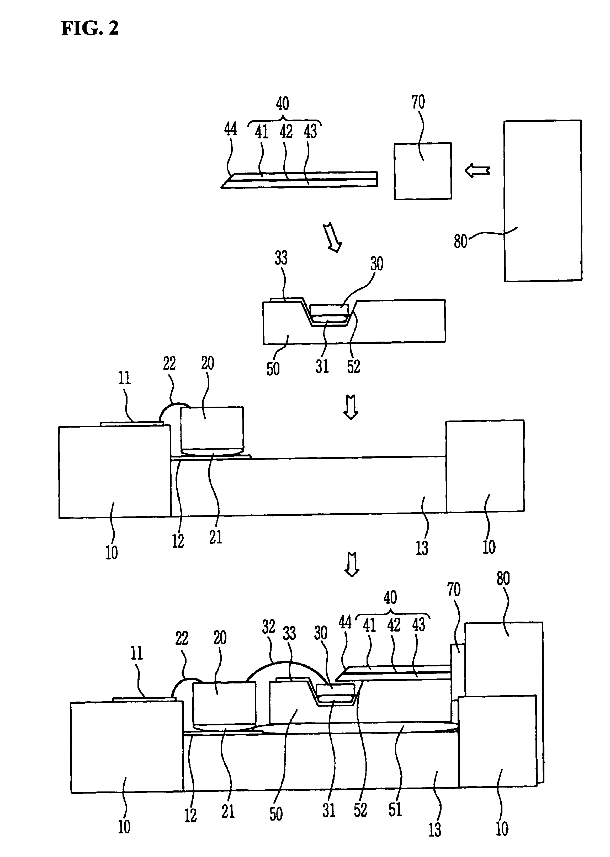
[0026]The present invention will be described in detail by way of a preferred embodiment with reference to accompanying drawings, in which like reference numerals are used to identify the same or similar parts.

[0027]Conventionally, a vertical cavity surface emitting laser (VCSEL) that can be available in a short wavelength band of 850 nm is used as a light source. In recent, however, as a vertical cavity surface emitting laser (VCSEL) that can be available in a long wavelength band of 1300 nm and 1550 nm has recently been developed, it is possible to implement a single mode vertical cavity surface emitting laser (VCSEL) optical transmit / receive module of a long wavelength. In addition, as the size of a core of a single mode optical waveguide is significantly made smaller compared to a multi-mode optical waveguide, there is a need for a new technology for optical interconnection and alignment with the vertical cavity surface emitting laser (VCSEL) and the photo diode (PD).

[0028]The p...


PUM


Abstract

The present invention relates to a parallel optical interconnection module for transmitting an optical signal over an optical fiber and receiving an optical signal from the optical fiber. According to the present invention, a reflection surface is formed at the end of the optical waveguide forming a core so that the path of light can be exactly changed and is focused. A light source/photodetector is buried within a trench using the silicon optical bench and an optical waveguide is manually aligned on the surface of the silicon optical bench, so that alignment error between the light source/photodetector and the optical waveguide can be minimized. A ferrule into which the optical waveguide is inserted is fixed to an adaptor so that alignment error between the optical waveguide and the light source/photodetector is minimized. Therefore, the present invention can minimize the coupling loss in the process during which the optical signal is transmitted to increase the optical output. Further, the present invention allows easy optical interconnection by means of a manual alignment and can increase the productivity.

Description

BACKGROUND OF THE INVENTION[0001]1. Field of the Invention[0002]The invention relates generally to a parallel optical interconnection module for transmitting an optical signal over an optical fiber and receiving an optical signal from the optical fiber, and method of manufacturing the same. More particularly, the present invention relates to a parallel optical interconnect optical transmit / receive module comprising an optical waveguide having a lens type reflection surface for reducing the coupling loss generated due to alignment error when it is coupled with an optical fiber, a silicon optical bench for reducing the coupling loss generated due to alignment error when it is coupled with the optical fiber, and a ferrule by which fixture to the optical waveguide for optical interconnection is facilitated.[0003]2. Description of the Prior Art[0004]Generally, in a low-speed system, or the like, interconnection between a circuit substrate and a circuit substrate, and a chip and a chip or...

Claims


Application Information

Patent Timeline
Patent Type & Authority Patents(United States)
IPC IPC(8): G02B6/42
CPCG02B6/42G02B6/421G02B6/4214H01L2224/48091H01L2224/48137H01L2224/73265H01L2924/3011H01L2924/00014H01L2924/00H01L2224/05554
Inventor HAN, SANG-PILCHOI, CHOON GIKIM, BYEONG CHEOLAHN, SEUNG HOCHO, IN KUIJEONG, MYUNG YUNG
Owner ELECTRONICS & TELECOMM RES INST
Why Eureka
Try Eureka