Electronic component

a technology of electronic components and components, applied in the field of electronic components, can solve problems such as the degradation of flexibility in the design of impedances, and achieve the effect of reducing the influence of an outer electrode and high design flexibility

Active Publication Date: 2019-01-29
MURATA MFG CO LTD
View PDF17 Cites 0 Cited by
  • Summary
  • Abstract
  • Description
  • Claims
  • Application Information

AI Technical Summary

Benefits of technology

[0009]Accordingly, the present invention is primarily directed to providing an electronic component that can reduce the influence of an outer electrode on the characteristics of an element and that has high flexibility in an impedance design.
[0011]Each of the outer electrodes is formed on a single side surface so as not to extend over two side surfaces of the multilayer body, and the first outer electrode connected to the first inner conductor and the second outer electrode connected to the second inner conductor are formed so as to have different shapes. Thus, an outer electrode does not need to be formed at a portion at which an internal electrode is not extended, and an outer electrode can be formed only at a necessary portion. Therefore, an area in which an outer electrode is formed can be kept to a minimum. Thus, a stray capacitance between an inner conductor and an outer electrode can be suppressed, and a parasitic inductance generated in an outer electrode can be suppressed. In addition, a situation in which a magnetic field generated in an inner conductor is blocked by an outer electrode can be suppressed, and an eddy-current loss generated in an outer electrode can be reduced.
[0017]As the first outer electrode connected to the first inner conductor, which serves as a ground electrode, is made longer in a direction intersecting with the direction in which the insulator layers are stacked, the isolation characteristics between the outer electrodes formed at respective sides of the first outer electrode can be improved.
[0019]Each of the outer electrodes is formed on a single side surface so as not to extend over two side surfaces of the multilayer body, and the first outer electrode and the second outer electrode are formed so as to reach one principal surface of the multilayer body but so as not to reach the other principal surface. Thus, an area in which an outer electrode is not formed can be provided in the direction in which the insulator layers are stacked. Therefore, a stray capacitance between an inner conductor and an outer electrode can be suppressed, and a parasitic inductance generated in an outer electrode can be suppressed. In addition, a situation in which a magnetic field generated in an inner conductor is blocked by an outer electrode can be suppressed, and an eddy-current loss generated in an outer electrode can be reduced.
[0021]As not only the first outer electrode and the second outer electrode but also all of the outer electrodes are formed so as to reach one principal surface of the multilayer body but so as not to reach the other principal surface, an effect of suppressing a stray capacitance and a parasitic inductance and an effect of suppressing a situation in which a magnetic field generated in an inner conductor is blocked can be enhanced.
[0028]According to the invention, an electronic component that can reduce the influence of an outer electrode on the characteristics of an element and that has the high design flexibility for obtaining the desired characteristics can be obtained.

Problems solved by technology

However, if different elements are to be connected to each outer electrode as in an LC composite component, for example, forming outer electrodes having an identical shape so as to extend from one principal surface to the other principal surface of an element assembly leads to such issues as the influence of a stray capacitance between an inner conductor and the outer electrodes, the influence of a parasitic inductance in the outer electrodes, an eddy-current loss caused as the outer electrodes block a magnetic field generated in the inner conductor, the interference among the outer electrodes, the degradation in the flexibility in an impedance design.

Method used


Image

  • Electronic component
  • Electronic component
  • Electronic component

Examples


Embodiment Construction

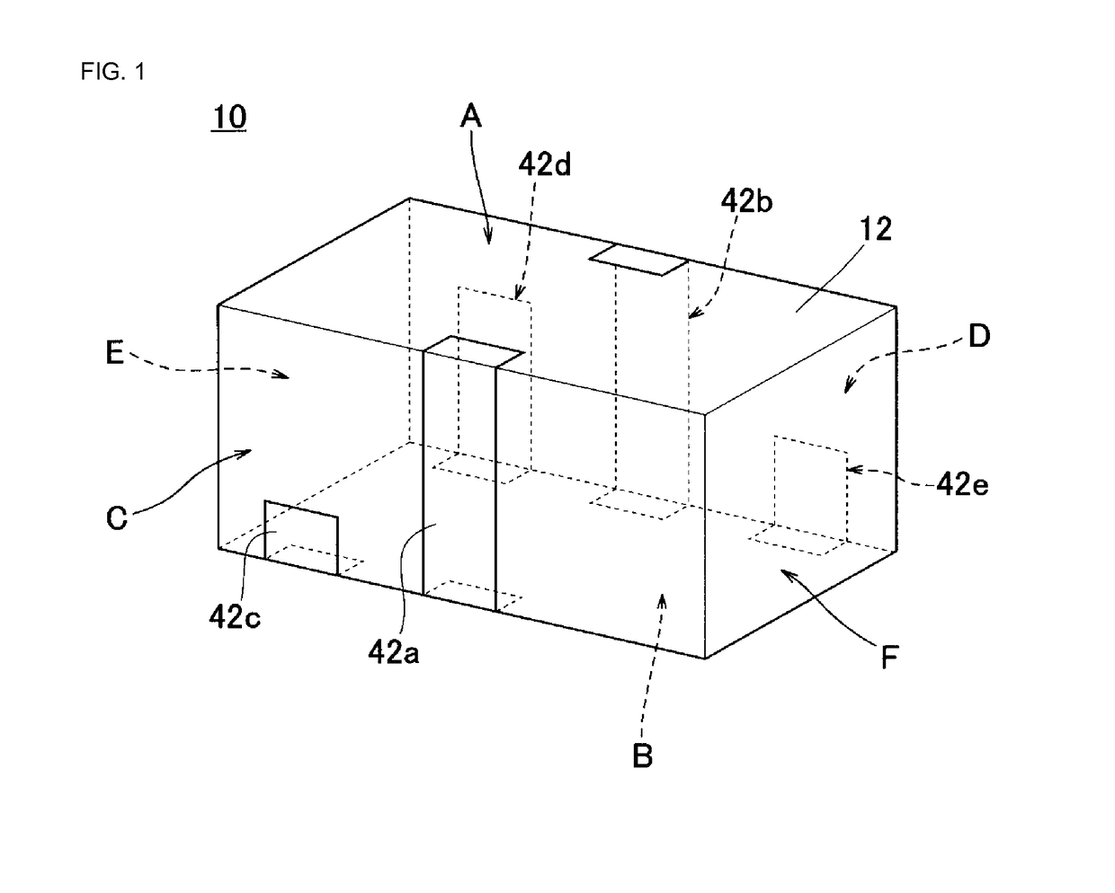
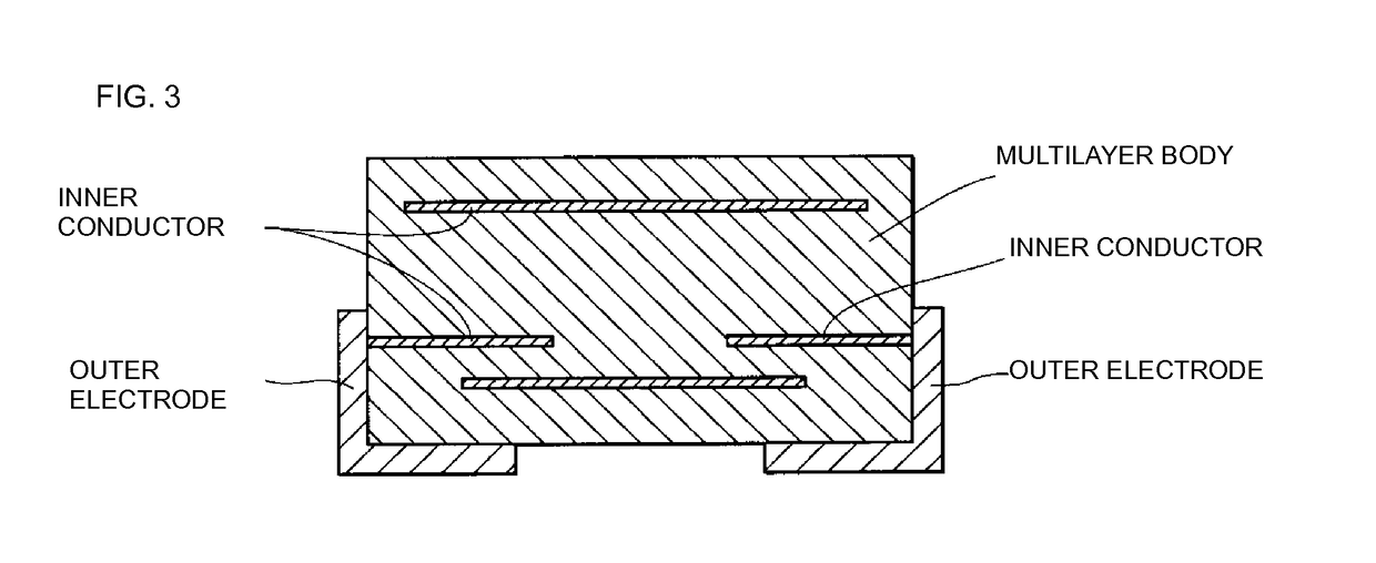
[0049]FIG. 1 illustrates a diplexer serving as an example of an electronic component according to the invention. An electronic component 10 includes a multilayer body 12. The multilayer body 12 is formed, for example, into a rectangular parallelepiped shape, and includes two rectangular principal surfaces (A-side and B-side) that are opposite to each other, a one-end-side side surface (C-side) and an another-end-side side surface (D-side) that are located at the sides of the two principal surfaces in the widthwise direction, and a one-end-side side surface (E-side) and an another-end-side side surface (F-side) that are located at the sides of the two principal surfaces in the lengthwise direction.

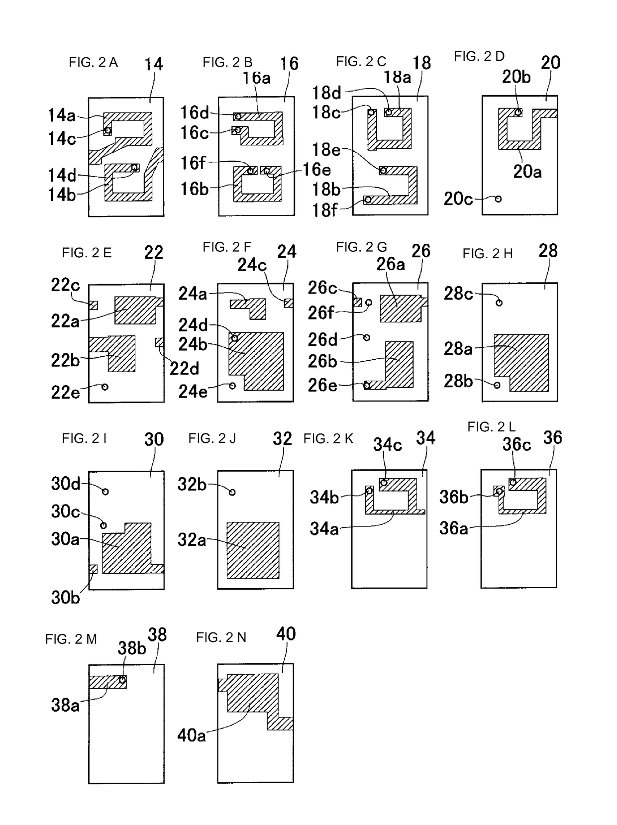
[0050]As illustrated in FIG. 2(A), the multilayer body 12 includes a first insulator layer 14 that is rectangular in shape. Two inner conductors 14a and 14b are formed on the first insulator layer 14. The inner conductor 14a is formed in an open ring shape on the first insulator layer 14 to...


PUM

PropertyMeasurementUnit
lengthaaaaaaaaaa
conductiveaaaaaaaaaa
insulatingaaaaaaaaaa

Abstract

A multilayer body 12 is obtained by stacking a plurality of insulator layers in which an inner conductor and a via hole conductor are formed. Outer electrodes 42a through 42e connected to the inner conductor layers are formed on the opposite side surfaces of the multilayer body 12. While the two outer electrodes 42a and 42b are formed so as to extend from one principal surface to the other principal surface of the multilayer body 12, the other outer electrodes 42c through 42e are formed so as to extend from one principal surface to an exposed portion of the inner conductor on the multilayer body 12, or formed so as not to reach the other principal surface. In addition, the widths of the outer electrodes 42a through 42e may differ from one another.

Description

BACKGROUND OF THE INVENTION[0001]Field of the Invention[0002]The present invention relates to electronic components, and relates in particular to an electronic component that includes an inner conductor formed between insulator layers forming a multilayer body and an outer electrode formed on a side surface of the multilayer body, for example.[0003]Description of the Related Art[0004]Examples of electronic components having a multilayer structure include, for example, a chip type CR composite array. FIG. 17 is a perspective view illustrating an example of an existing chip type CR composite array, and FIG. 18 is an exploded perspective view of an element assembly used in the chip type CR composite array. A chip type CR composite array 1 includes an element assembly 2 having a multilayer structure. The element assembly 2 is formed by stacking a plurality of insulator layers 3. An inner ground electrode 4 and four resistive bands 5 are formed so as to sandwich one of the insulator laye...

Claims


Application Information

Patent Timeline
Patent Type & Authority Patents(United States)
IPC IPC(8): H01F5/00H01F27/28H01F17/00H01F27/29H01G4/232H01G4/30
CPCH01F27/2804H01F17/0013H01F27/292H01G4/30H01F2027/2809H01G4/232
Inventor MATSUSHITA, YOSUKEOKANO, TAKAOSASAKI, HIROYUKIKIKUCHI, KENICHIRO
Owner MURATA MFG CO LTD
Why Eureka
Try Eureka