High-frequency module

a high-frequency module and module technology, applied in the direction of final product manufacturing, sustainable manufacturing/processing, semiconductor/solid-state device details, etc., can solve the problems of increasing the number of manufacturing steps of the terminal connection substrate b>103/b>, stress is subject to, and the connection reliability of the module mounted on the external substrate can be increased, and damage may be caused. , the effect of dispersing stress

Active Publication Date: 2020-12-17
MURATA MFG CO LTD
View PDF0 Cites 0 Cited by
  • Summary
  • Abstract
  • Description
  • Claims
  • Application Information

AI Technical Summary

Benefits of technology

[0012]According to such a configuration, the third terminal assembly in which the external connection terminals are aligned at small intervals is mounted on a portion of a substrate, to which stress is likely to be applied, so that the external connection terminals are arranged closer to one another, and such stress can thereby be dispersed. Thus, the connection reliability when the module is mounted on the external substrate can be increased.
[0013]When the module is mounted on the external substrate, stress is likely to be applied especially to the corner portion of the substrate and damage may be caused. However, the connection strength can be increased by dispersing such stress by mounting the third terminal assembly on the corner portion of the substrate and arranging the external connection terminals closer to one another.
[0014]In addition, the resin block may be made of a resin having a dielectric loss tangent smaller than a dielectric loss tangent of a resin that forms the first sealing resin layer. According to such a configuration, the resin used for the sealing resin layer has a low dielectric characteristic (permittivity or the dielectric loss tangent is large), and stray capacitance between the external connection terminals is thereby likely to be formed in a high-frequency range and signal loss thus increases. However, the stray capacitance between the external connection terminals can be reduced by forming the resin block by using a resin having a small dielectric loss tangent, and signal loss can thus be reduced.
[0015]In addition, a component mounted on another main surface of the circuit board, and a second sealing resin layer configured to cover the other main surface of the circuit board and the component may further be included. According to such a configuration, it is possible to provide the module that is a double-sided-mounting type and has high connection reliability.
[0016]According to the present disclosure, the bonding reliability after the module is mounted on the external substrate can be increased by increasing the size of the external connection terminal positioned in the corner portion of the substrate that is easily subjected to stress when the module is mounted on the external substrate.

Problems solved by technology

However, when the above-described module substrate 100 is mounted on an external substrate, the terminal electrodes 111 positioned in four-corner portions of the base substrate 101 are subjected to stress and thus tend to be easily damaged.
In such a case, although a method in which connection strength is increased by increasing the size of the terminal electrodes 111 positioned in the four-corner portions of the base substrate 101 can be considered, to form the terminal connection substrate 103 by arranging the terminal electrodes 111 having different diameters in one terminal connection substrate 103, there is a problem that the number of manufacturing steps of the terminal connection substrate 103 increases and costs increase.

Method used


Image

  • High-frequency module
  • High-frequency module
  • High-frequency module

Examples


Embodiment Construction

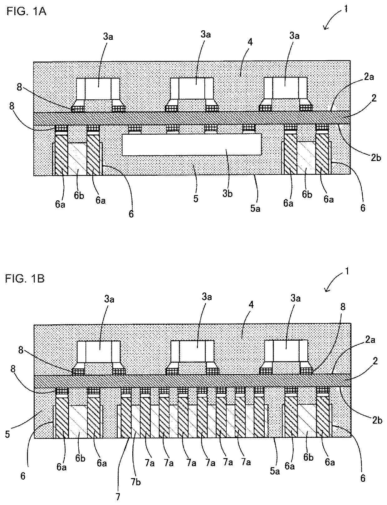
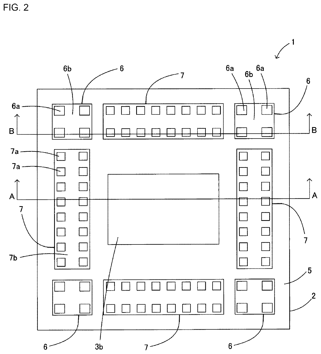
[0026]A high-frequency module 1 according to an embodiment of the present disclosure will be described with reference to FIGS. 1A, 1B and 2. In FIGS. 1A and 1B, FIG. 1A is a sectional view of the high-frequency module 1 according to Embodiment 1 in FIG. 2 taken along line A-A, and FIG. 1B is a sectional view of the high-frequency module 1 in FIG. 2 taken along line B-B. FIG. 2 is a plan view of the high-frequency module 1.

[0027]As FIGS. 1A, 1B and 2 illustrate, the high-frequency module 1 according to the present embodiment includes a substrate 2 having an upper surface 2a (corresponding to “another main surface” of the present invention) and a lower surface 2b (corresponding to “one main surface” of the present invention). A plurality of components 3a are mounted on the upper surface 2a, and a component 3b is mounted on the lower surface 2b. A second sealing resin layer 4 is stacked on the upper surface 2a, and a first sealing resin layer 5 is stacked on the lower surface 2b. The h...


PUM


Abstract

A high-frequency module 1 includes a component 3a mounted on an upper surface 2a of a substrate 2, a second sealing resin layer 4 stacked on the upper surface 2a of the substrate 2, a component 3b mounted on a lower surface 2b of the substrate 2, a first sealing resin layer 5 stacked on the lower surface 2b of the substrate 2, and a first terminal assembly 6 and a second terminal assembly 7 that are mounted on the lower surface 2b of the substrate 2. The first terminal assembly 6 is mounted on a four-corner portion of the substrate 2 and includes a connection conductor 6a thicker than a connection conductor 7a of the second terminal assembly 7.

Description

[0001]This is a continuation of International Application No. PCT / JP2019 / 010729 filed on Mar. 15, 2019 which claims priority from Japanese Patent Application No. 2018-052670 filed on Mar. 20, 2018. The contents of these applications are incorporated herein by reference in their entireties.BACKGROUND OF THE DISCLOSUREField of the Disclosure[0002]The present disclosure relates to a high-frequency module in which a terminal assembly is mounted.Description of the Related Art[0003]A method for manufacturing a module including an interlayer connection conductor at low cost in a short manufacturing time by mounting a terminal connection substrate, in which a plurality of columnar terminal electrodes are connected to one another with an insulator interposed therebetween, on a module substrate has been proposed, and Patent Document 1 proposes such a method. For example, regarding a module substrate 100 illustrated in FIG. 9, electronic components 102 are mounted on surface electrodes of an u...

Claims


Application Information

Patent Timeline
Patent Type & Authority Applications(United States)
IPC IPC(8): H05K1/02H01L23/66H05K1/18
CPCH05K1/181H01L23/66H05K1/0243H01L2223/6605H01L23/12H05K1/144H05K2201/10424H05K3/288H05K2203/025H05K3/284H05K2203/1316H05K2203/175H05K2203/176H01L2224/16227H01L2224/131H01L2924/19042H01L2924/19041H01L25/16H01L25/065H01L2224/97H01L2224/81815H01L2924/30105H01L23/552H01L2924/3025H01L23/49833H01L24/13H01L24/16H01L24/81H01L24/97H01L23/49811H01L21/4853H01L23/3121Y02P70/50H01L2924/014H01L2924/00014H01L2224/81
Inventor BANBA, SHINICHIRO
Owner MURATA MFG CO LTD
Why Eureka
Try Eureka