High aspect ratio openings

a high aspect ratio, opening technology, applied in the direction of fixed capacitor details, capacitor manufacture, fixed capacitors, etc., can solve the problems of tapered profile, less effective etching, and difficulty in obtaining

Inactive Publication Date: 2012-09-25
MICRON TECH INC
View PDF273 Cites 47 Cited by
  • Summary
  • Abstract
  • Description
  • Claims
  • Application Information

AI Technical Summary

Problems solved by technology

Its sputtering nature creates difficulty in obtaining a straight profile since the etch does not exhibit a lateral component, leading to a tapered profile.
In addition to tapered etch profiles, use of silicon dioxide also may produce feature charging due to its insulative nature.
As a result, as aspect ratio increases, etching may become less effective.
Features across a surface being etched might not be symmetrical, resulting in feature charging differences in lateral directions.
Photo irregularities become apparent on inspection after the development step during photolithography.
The twisting phenomenon with respect to HAR openings is problematic in that twisting reduces the efficiency of a contact by increasing the distance between active device areas and by increasing the difficulty of filling a contact with a conductive material, or can weaken or distort vertical structures formed by etching.
Such twisting may cause electrical opens when the opening misses a landing contact, or may cause electrical shorts when the opening twists into an adjacent feature, or may cause unwanted variations in deposition layers upon distorted vertical structures.

Method used


Image

  • High aspect ratio openings
  • High aspect ratio openings
  • High aspect ratio openings

Examples


Embodiment Construction

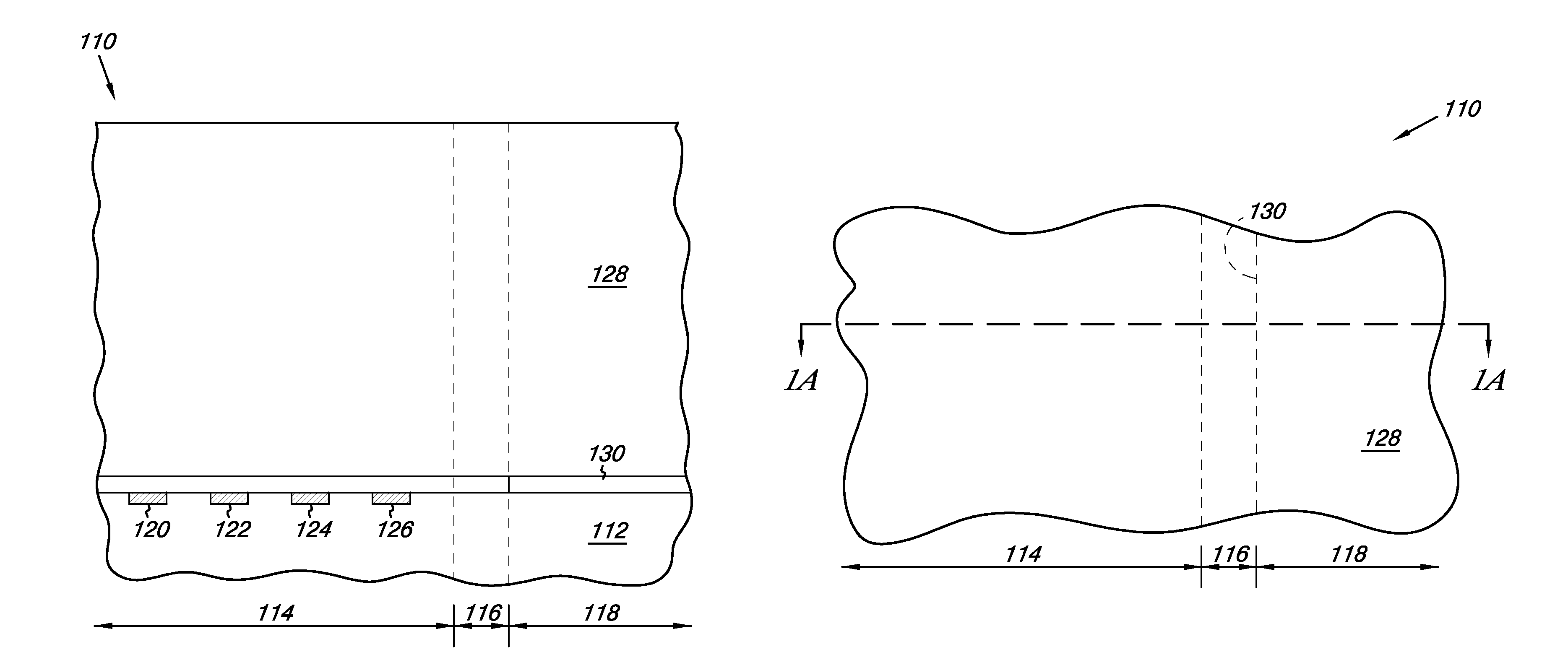
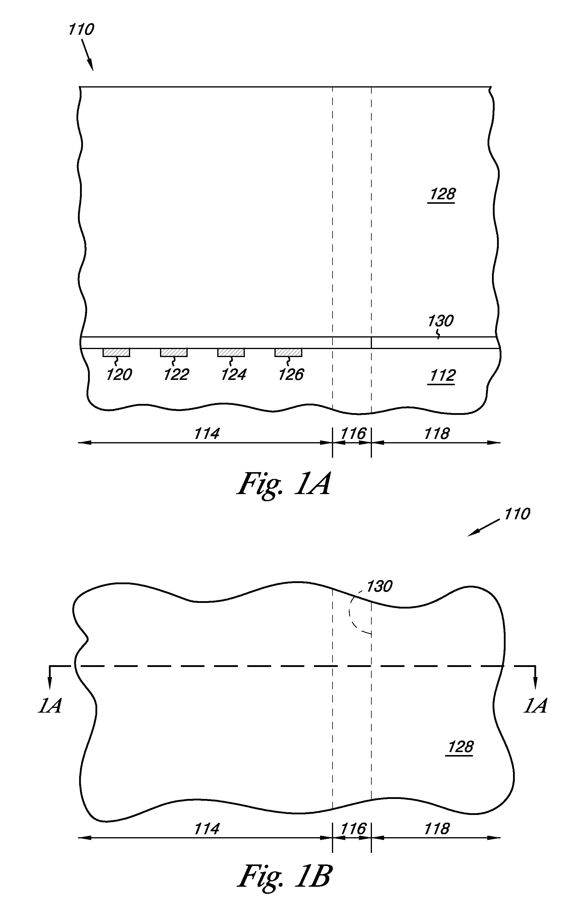
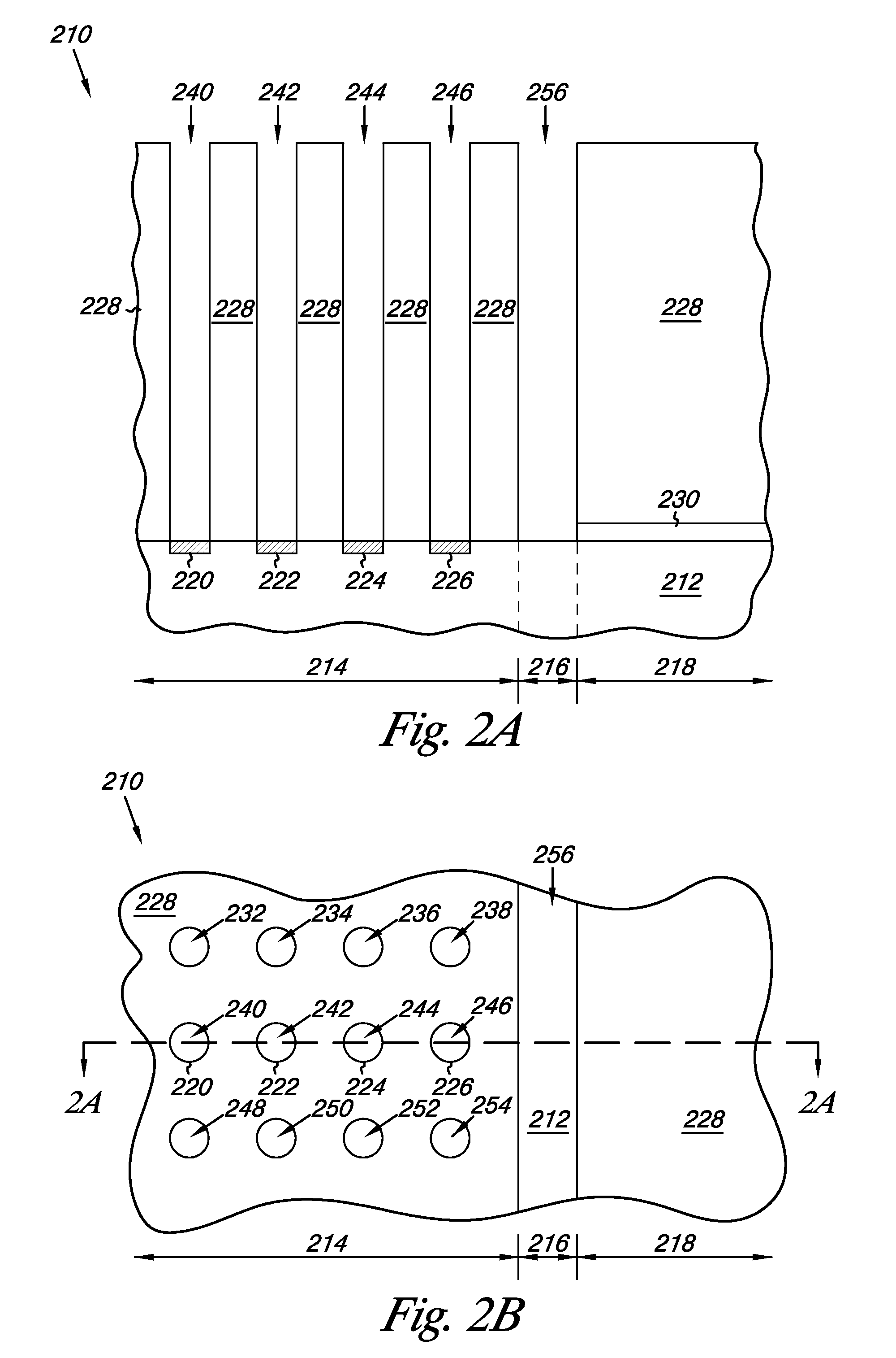
[0023]The present disclosure includes methods, capacitors, and high aspect ratio (HAR) structures, e.g., openings, vertical features. One method embodiment of a capacitor forming method includes forming an electrically conductive support material over a substrate, with the support material containing at least 25 atomic percent (at %) carbon. The method includes forming an opening through at least the support material where the opening has an aspect ratio of at least 20:1 within a thickness of the support material. After forming the opening, the method includes processing the support material to effect a reduction in conductivity, and forming a capacitor structure in the opening.

[0024]In memory devices and other semiconductor-based circuitry, capacitors, e.g., MBit capacitors, are typically etched into substrates, followed by deposition of cell plates and dielectrics, e.g., charge-separating layers. In previous approaches, fabrication of capacitors includes formation in dielectric fi...


PUM

PropertyMeasurementUnit
temperatureaaaaaaaaaa
thicknessaaaaaaaaaa

Abstract

A capacitor forming method includes forming an electrically conductive support material over a substrate, with the support material containing at least 25 at % carbon. The method includes forming an opening through at least the support material where the opening has an aspect ratio of at least 20:1 within a thickness of the support material. After forming the opening, the method includes processing the support material to effect a reduction in conductivity, and forming a capacitor structure in the opening.

Description

TECHNICAL FIELD[0001]The invention relates to semiconductors and semiconductor fabrication methods. More particularly, the invention relates to high aspect ratio openings and etching methods for formation of high aspect ratio openings.BACKGROUND[0002]Openings are formed in support materials so that microelectronic structures may be formed in and their structure supported by the support material. For example, a capacitor container for a dynamic random access memory (DRAM) cell may be etched into a dielectric, such as silicon dioxide (SiO2), which can be formed as a doped silicate glass. Use of silicon dioxide dielectric can yield several disadvantages from an etching standpoint. Dry etch of silicon dioxide has a large physical component, that is, it is more like physical sputtering than like a chemical etch. Its sputtering nature creates difficulty in obtaining a straight profile since the etch does not exhibit a lateral component, leading to a tapered profile.[0003]The profile of an...

Claims


Application Information

Patent Timeline
Patent Type & Authority Patents(United States)
IPC IPC(8): H01G4/00
CPCH01L27/10894H01L27/10817H01G4/08H01L27/10852H01L28/40H01G13/00Y10T29/43H01G4/33H01G4/012H01L28/90H10B12/318H10B12/09H10B12/033
Inventor KIEHLBAUCH, MARK W.
Owner MICRON TECH INC
Why Eureka
Try Eureka