
Trimming circuit of semiconductor memory apparatus and trimming method thereof

a semiconductor memory and circuit technology, applied in emergency protective devices, heating/cooling contact switches, instruments, etc., can solve the problem of insufficient precision in trimming internal voltage, and achieve the effect of efficient trimming internal voltag

Active Publication Date: 2012-10-02
SK HYNIX INC
View PDF9 Cites 9 Cited by
  • Summary
  • Abstract
  • Description
  • Claims
  • Application Information

AI Technical Summary

Benefits of technology

The patent describes a trimming circuit for a semiconductor memory apparatus that can efficiently trim internal voltage. The circuit includes a trimming code generator and an internal voltage generator. The trimming code generator generates a trimming code signal group by performing addition or subtraction using a test mode signal and a fuse coding signal. The internal voltage generator provides trimmed voltage in response to the trimming code signal group as output voltage. The circuit can also include multiple internal voltage generators, a test mode controller, and a calculator block to selectively provide a trimming code signal group based on the voltage control signals. The method involves providing a fuse coding signal, decoding the test mode signal, and performing addition and subtraction operations to generate the trimming code signal group. The technical effect of this patent is to provide a more efficient and precise way to trim internal voltage in a semiconductor memory apparatus.

Problems solved by technology

However, when the trimming is required after a package process, the trimming for the internal voltage may not be precisely performed even if a code signal is used since a preset base voltage is primarily trimmed when the trimming operation is performed in a package level.

Method used


Image

  • Trimming circuit of semiconductor memory apparatus and trimming method thereof
  • Trimming circuit of semiconductor memory apparatus and trimming method thereof
  • Trimming circuit of semiconductor memory apparatus and trimming method thereof

Examples


Embodiment Construction

.”

BRIEF DESCRIPTION OF THE DRAWINGS

[0014]Features, aspects, and embodiments are described in conjunction with the attached drawings, in which:

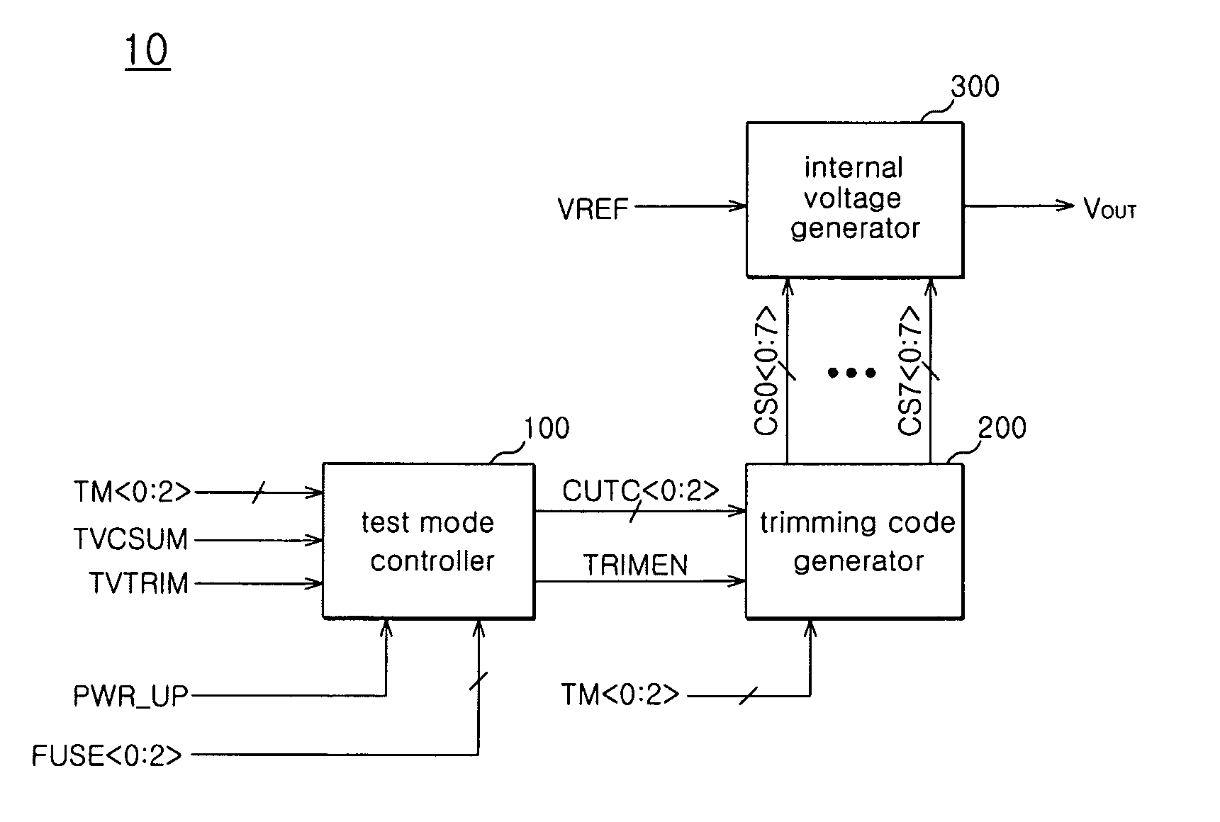
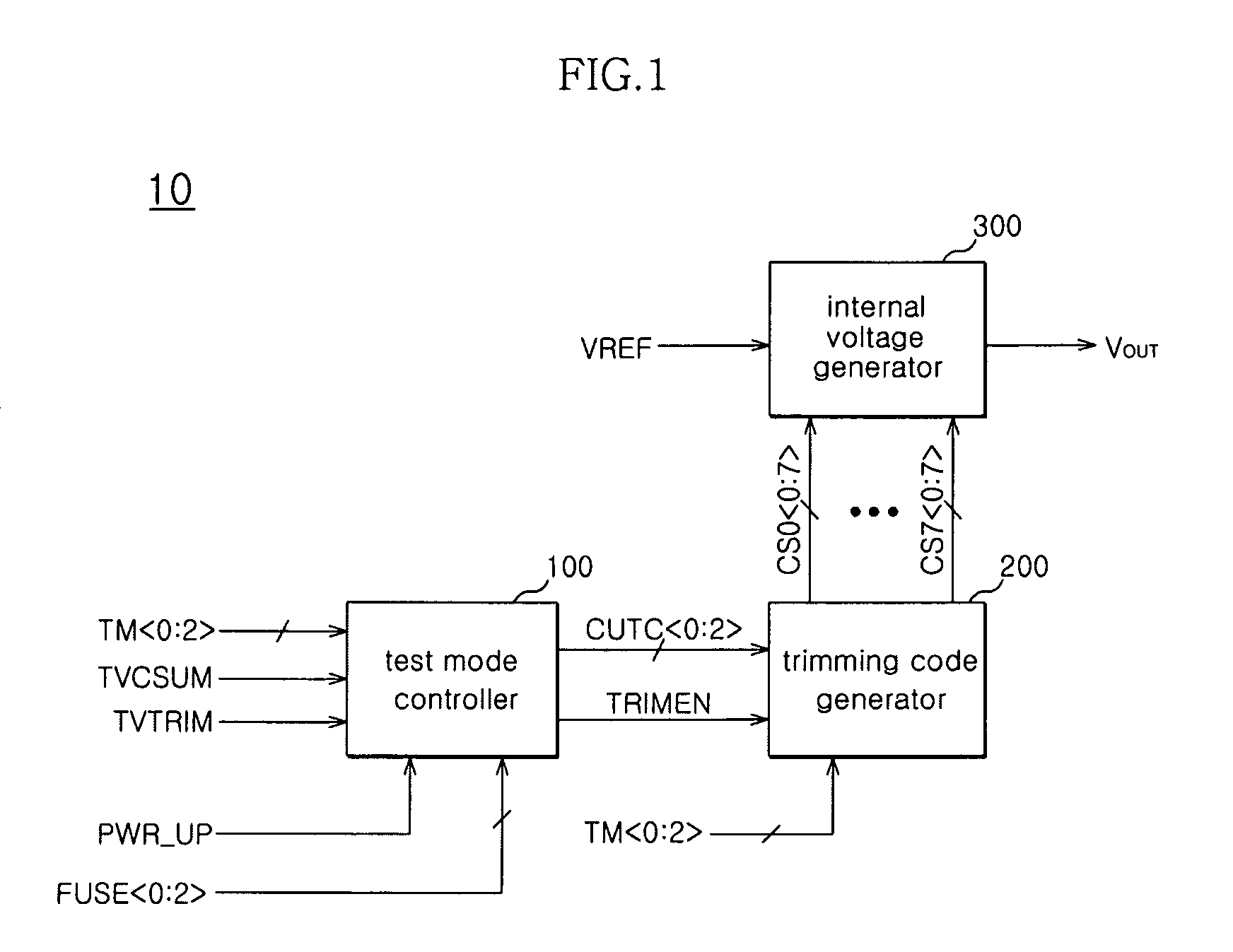
[0015]FIG. 1 is a schematic block diagram of an exemplary trimming circuit for a semiconductor memory apparatus according to one embodiment;

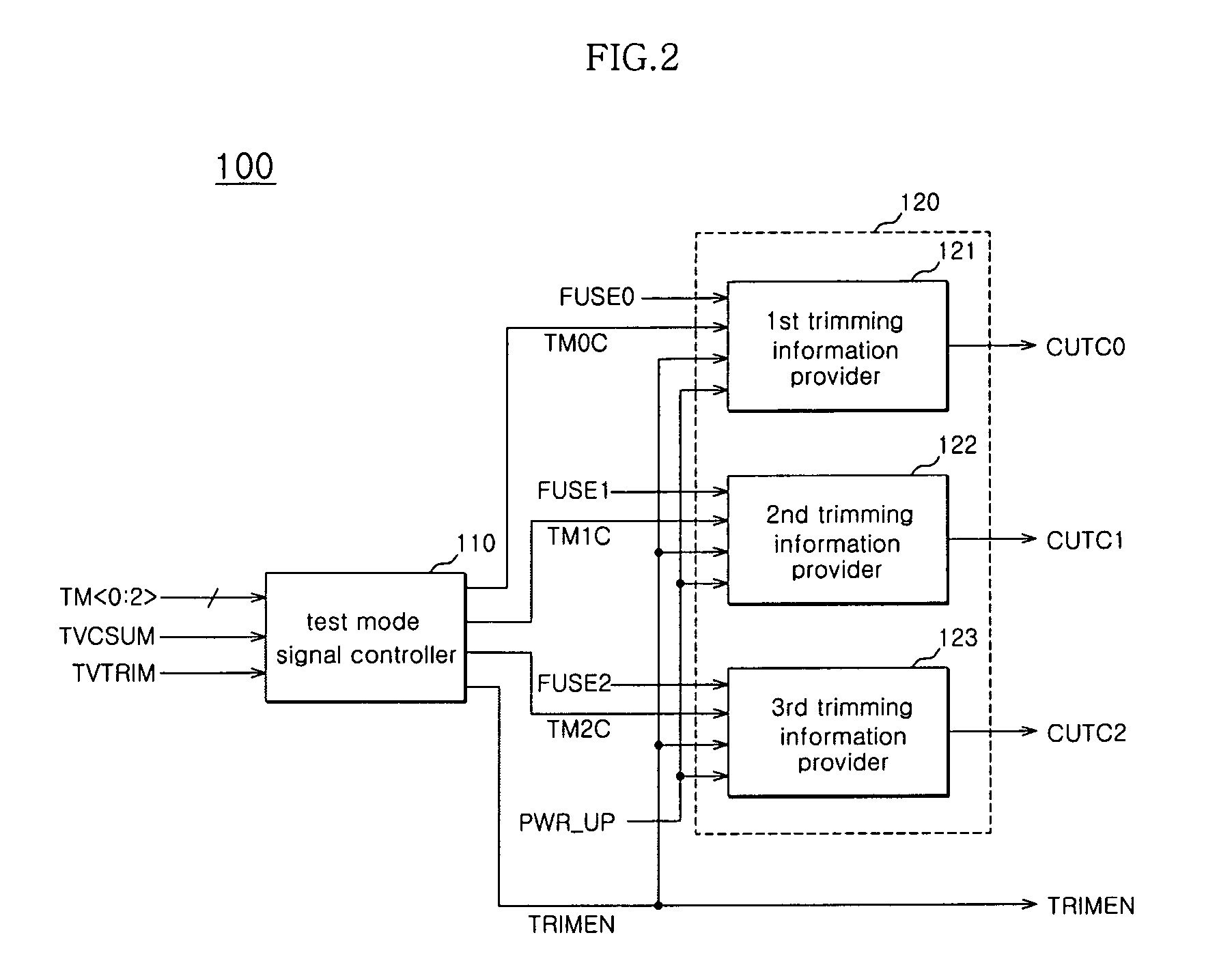
[0016]FIG. 2 is a schematic block diagram of an exemplary test mode controller capable of being implemented in the circuit of FIG. 1 according to one embodiment;

[0017]FIG. 3 is a schematic diagram of an exemplary circuit for the test mode signal controller of FIG. 2 according to one embodiment;

[0018]FIG. 4 is a schematic circuit diagram of an exemplary first trimming information provider capable of being implemented in the trimming information block of FIG. 2 according to one embodiment;

[0019]FIG. 5 is a schematic block diagram of an exemplary trimming code generator capable of being implemented in the circuit of FIG. 1 according to one embodiment;

[0020]FIG. 6 is a schematic circuit diagram of an exemplary...


PUM


Abstract

A trimming circuit for a semiconductor memory apparatus includes a trimming code generator configured to provide a trimming code signal group by performing one of addition and subtraction using a test mode signal and a fuse coding signal, and an internal voltage generator configured to provide trimmed voltage in response to the trimming code signal group as output voltage.

Description

CROSS-REFERENCES TO RELATED APPLICATION[0001]The present application claims priority under 35 U.S.C. 119(a) to Korean application number 10-2008-0100549, filed on Oct. 14, 2008, in the Korean Intellectual Property Office, which is incorporated herein by reference in its entirety as if set forth in full.BACKGROUND[0002]1. Technical Field[0003]The embodiments described herein relate to a semiconductor memory apparatus, and more particularly, to a trimming circuit for a semiconductor memory apparatus.[0004]2. Related Art[0005]In general, since external supply voltages or ground voltages may have instant variations in noise and voltage levels, a circuit in a semiconductor memory apparatus requires voltages having a stable level. Accordingly, the semiconductor memory apparatus generates internal voltages having various levels by using an external supply voltage or a ground voltage.[0006]The semiconductor memory apparatus includes an internal voltage generating circuit to generate interna...

Claims


Application Information

Patent Timeline
Patent Type & Authority Patents(United States)
IPC IPC(8): G06F19/00H01H37/76
CPCG11C17/18G11C29/02G11C29/021G11C29/028G11C16/04G11C7/22G11C5/14G11C29/04
Inventor KIM, JEE-YUL
Owner SK HYNIX INC
Learn More