Signal processor comprising an amplifier

a signal processor and amplifier technology, applied in the field of signal processing, can solve the problems of significant distortion component, non-negligible tail current modulation characteristic, and substantially nonlinearity, and achieve the effects of reducing distortion, reducing imbalance in the pair of complementary, and reducing offset output curren

Active Publication Date: 2012-10-16
NXP BV
View PDF6 Cites 8 Cited by
  • Summary
  • Abstract
  • Description
  • Claims
  • Application Information

AI Technical Summary

Benefits of technology

[0008]Another advantage of the invention relates to the following aspects. In principle, it is possible to reduce distortion by reducing the imbalance in the pair of complementary differential pairs. The smaller the imbalance is, the smaller the offset output current is. The smaller the offset output current is, the smaller the distortion component is for a given tail current modulation characteristic. The tail current modulation characteristic is substantially linear in an amplifier according to the invention, whereas the tail current modulation characteristic is substantially nonlinear in the prior art amplifier. Consequently, an amplifier according to the invention can tolerate a significantly greater degree of imbalance than the prior art amplifier, if a given distortion requirement should be met. Stated otherwise, the prior art amplifier tolerates only a relatively small degree of imbalance from a distortion point of view. Achieving a relatively small degree of imbalance requires relatively precise manufacturing techniques or relatively large components, or both, which entails relatively high cost. Since an amplifier in accordance with the invention tolerates a relatively great degree of imbalance, the invention allows low-cost implementations.
[0009]An implementation of the invention advantageously comprises one or more of following additional features, which are described in separate paragraphs that correspond with individual dependent claims.
[0010]In each aforementioned differential pair, the biasing circuit that provides the tail current is preferably in the form of a resistance. This further contributes to achieving a relatively low distortion at modest cost.
[0011]The current combining circuit preferably comprises a pair of current-inverting buffers. Each current-inverting buffer comprises an input node that is coupled to a first supply voltage line via a biasing circuit for applying a bias current to the input node. The one and the other current-inverting buffer receive an output current and a complementary output current, respectively, of one differential pair at their respective input nodes. The current combining circuit further comprises a current mirror for mirroring an output current of one current-inverting buffer. The current mirror comprises an input branch and an output branch, each branch including a transistor having a main terminal that is coupled to a second supply voltage line via an impedance. The input branch and the output branch receive an output current and a complementary output current, respectively, of the other differential pair at the respective main terminals of the respective transistors. An output node receives an output current of the other current-inverting buffer and an output current of the current mirror. These features further contribute to achieving low distortion for relatively large input signals.
[0012]In each aforementioned current-inverting buffer, the biasing circuit that applies the bias current to the input node is preferably in the form of a resistance. This further contributes to achieving to achieving low distortion for relatively large input signals.
[0013]Each aforementioned current-inverting buffer comprises preferably comprises a transistor having a control terminal coupled to receive a bias voltage and a main terminal that constitutes the input node of the current-inverting buffer.

Problems solved by technology

In practice, the prior-art topology will produce an offset output current, which is due to imbalance in the differential input stages.
However, the tail current modulation characteristic is non-negligible and, moreover, substantially nonlinear when common mode voltages vary in a relatively large range between signal ground and the supply voltage.
This nonlinear modulation, which occurs when relatively large common mode input signals are present, will produce a significant distortion component.

Method used


Image

  • Signal processor comprising an amplifier
  • Signal processor comprising an amplifier
  • Signal processor comprising an amplifier

Examples


Embodiment Construction

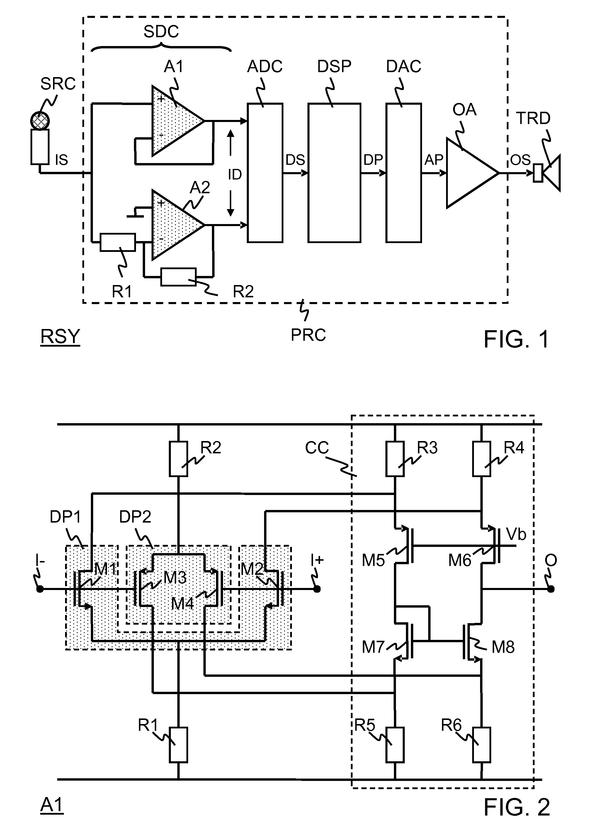
[0021]FIG. 1 illustrates a signal rendering system RSY that comprises a signal source SRC, a signal processor PRC, and a signal transducer TRD. The signal source SRC may be in the form of, for example, a microphone. The signal transducer TRD may be in the form of, for example, a loudspeaker. The signal processor PRC may be implemented in the form of, for example, an integrated circuit.

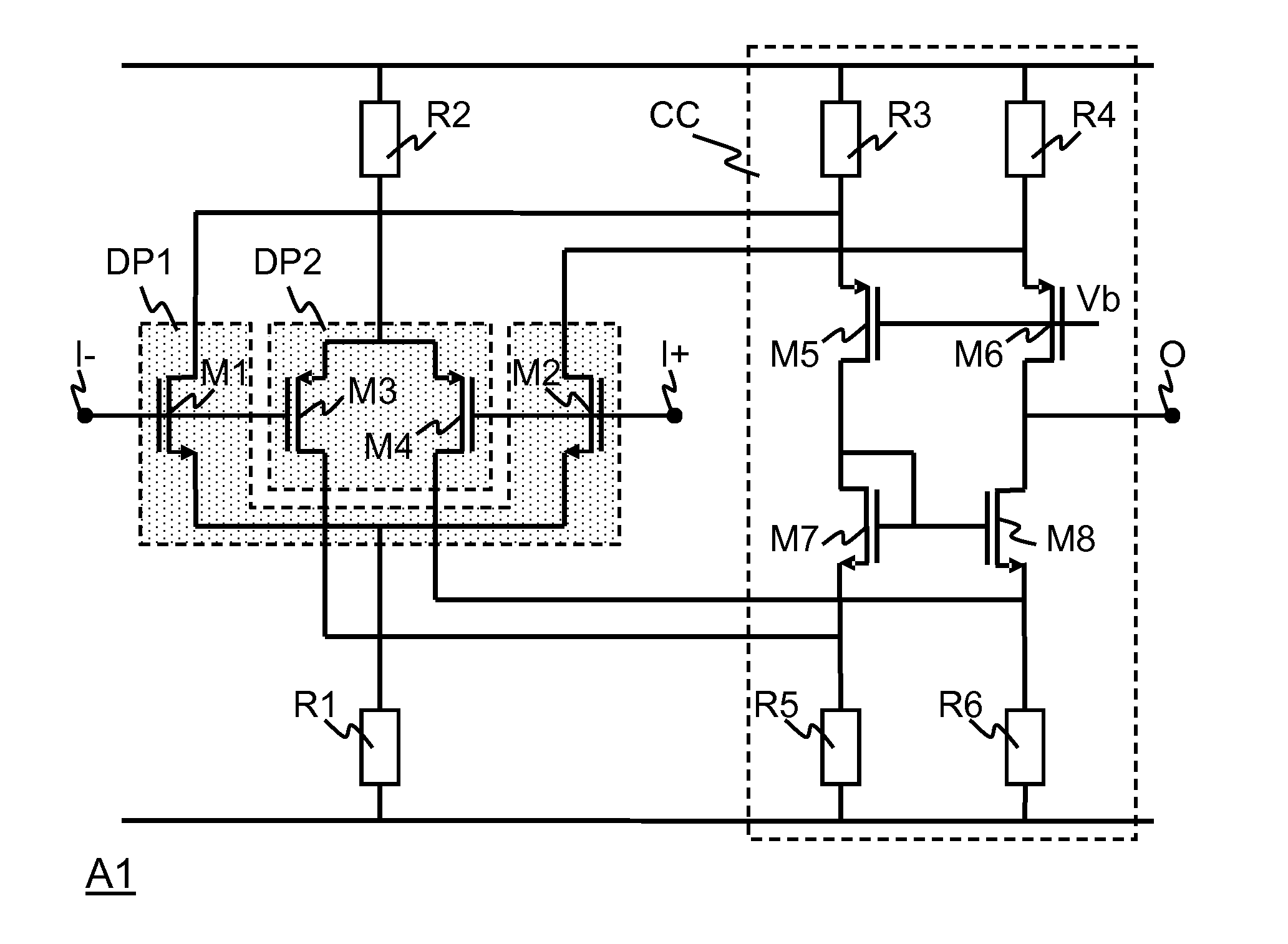
[0022]In more detail, the signal processor PRC comprises a single-ended to differential converter SDC, an analog-to-digital converter ADC, a digital signal processor DSP, a digital to analog converter DAC, and an output amplifier OA. The single-ended to differential converter SDC comprises two amplifiers A1, A2. Each amplifier has an inverting input +, a non-inverting input −, and an output. Amplifiers A1 operates as a non-inverting buffer by means of a short circuit between the output and the inverting input. This amplifier A1 will be referred to as non-inverting amplifier A1 hereinafter. The non-inve...


PUM


Abstract

An amplifier (A1) within a signal processor comprises a pair of complementary differential pairs (DP1, DP2) in the sense that one differential pair comprises transistors having a polarity opposite to that of transistors in the other differential pair. The one and the other differential pair commonly receive a differential input signal, which has a common mode component. A current combining circuit (CC) combines output currents of the one and the other differential pair so as to obtain an output current that varies as a function of the differential input signal. The one and the other differential pair each have a biasing circuit (R1, R2), which provides a tail current that varies with the common mode component in a substantially linear fashion.

Description

FIELD OF THE INVENTION[0001]An aspect of the invention relates to a signal processor that includes an amplifier, which comprises a pair of complementary differential pairs coupled to commonly receive a differential input signal. The signal processor may be implemented in the form of, for example, an integrated circuit. Another aspect of the invention relates to a signal rendering system.BACKGROUND OF THE INVENTION[0002]The article entitled “Low-Power Low-Voltage VLSI Operational Amplifier Cells” by Johan H. Huijsing et al., published in IEEE Transactions on Circuits and Systems, Vol. 42, No. 11, November 1995, describes voltage-efficient input stages (section II). The following considerations are made. A P-channel differential CMOS input stage has a common mode input voltage range that extends from a negative rail voltage up to a positive rail voltage minus a gate-source voltage VGS and a saturation voltage VDsat of a tail-current source. A N-channel differential CMOS input stage ha...

Claims


Application Information

Patent Timeline
Patent Type & Authority Patents(United States)
IPC IPC(8): H03F3/45
CPCH03F3/4521H03F2203/45498
Inventor BRUIN, PAULUS P. F. M.
Owner NXP BV
Why Eureka
Try Eureka