Unlock instant, AI-driven research and patent intelligence for your innovation.

Semiconductor device and data processing system having a reduced number of terminals allocated for externally accessed address

a technology of a semiconductor device and a data processing system, which is applied in the direction of memory address allocation/allocation/relocation, instruments, etc., can solve the problem of not being able to assign address terminals in a number equal to the number of bits of a connection, and achieve the effect of reducing the number of external terminals allocated for address input to receive access from outside, reducing the delay of address generation operation, and improving system efficiency

Inactive Publication Date: 2012-10-16
RENESAS ELECTRONICS CORP
View PDF6 Cites 2 Cited by
  • Summary
  • Abstract
  • Description
  • Claims
  • Application Information

AI Technical Summary

Benefits of technology

The present invention provides a semiconductor device with a reduced number of external terminals allocated for address input to receive access from outside. This allows for a high-speed response to external accesses and improves system efficiency in terms of resource usage efficiency and reduction of system cost. The semiconductor device includes an external interface circuit with supplementary register, mode register, and address control circuit to generate an address signal based on information input from external terminals, required supplementary information, and mode information of the mode register. The address information can be supplemented using the preliminary set in the supplementary register, without requiring processing such as decoding, resulting in a small delay in address generation. The invention allows for many variations in address generation form using a small number of external terminals.

Problems solved by technology

If a 32-Bit address signal, for example, is required to freely access an address space of a processor, it is often impossible to assign address terminals in a number equal to the number of bits to a connection for allowing the external device to access resources of the processor due to limitation of the number of external terminals.

Method used


Image

  • Semiconductor device and data processing system having a reduced number of terminals allocated for externally accessed address
  • Semiconductor device and data processing system having a reduced number of terminals allocated for externally accessed address
  • Semiconductor device and data processing system having a reduced number of terminals allocated for externally accessed address

Examples


Embodiment Construction

[0034]1. Outline of Embodiments

[0035]First, representative embodiments of the invention disclosed in this application are outlined. Reference numerals of the drawings which are referred to in parentheses in the outline explanation of the representative embodiments merely exemplify what are included in the concept of the components to which the numerals are provided.

[0036][1]

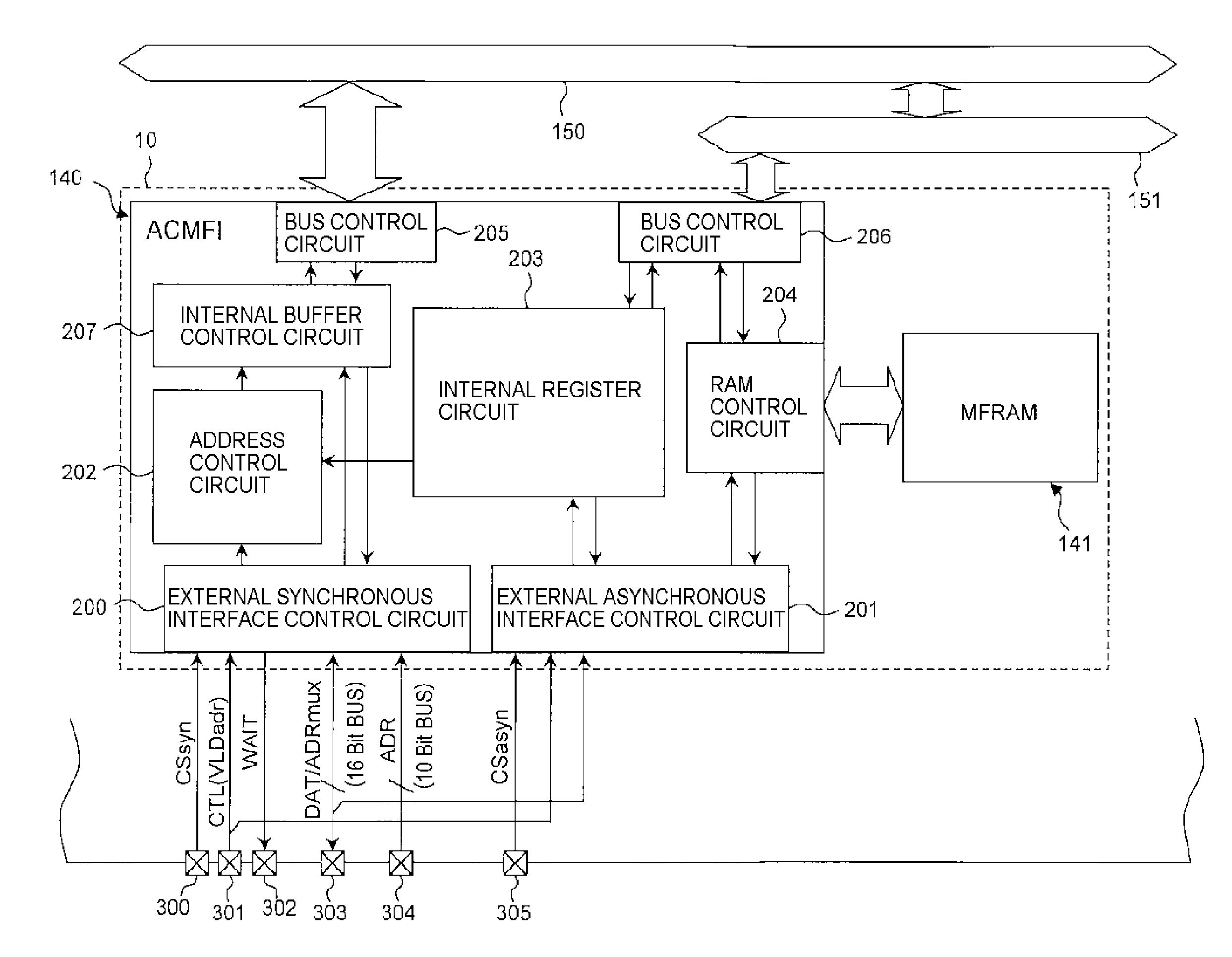
[0037]A semiconductor device (2) according to a representative embodiment of the present invention comprises a data processing unit (100), and an external interface circuit (10) which controls access to an address space of the data processing unit from outside the semiconductor device. The external interface circuit comprises a plurality of external terminals (303,304) for inputting, from outside the semiconductor device, a part of an address signal used to access the address space, a supplementary register (401) in which supplementary information (complementary information) for supplementing an upper portion of ...


PUM


Abstract

There is provided a semiconductor device having a reduced number of external terminals allocated for address input to receive access from outside, while realizing a high-speed response to an access from outside.The semiconductor device employs, in order to allow other external devices to directly access resources it possesses in its own address space, in an external interface circuit, external terminals which input a part of the address signal required for access from outside, a supplementary register which supplements the upper portion of address information that has been input from the external terminals, a mode register accessible from outside, and an address control circuit which generates an address signal to access the address space in a form based on information input from the external terminals, required supplementary information, and mode information of the mode register.

Description

CROSS-REFERENCE TO RELATED APPLICATION[0001]The disclosure of Japanese Patent Application No. 2010-38857 filed on Feb. 24, 2010 including the specification, drawings and abstract is incorporated herein by reference in its entirety.BACKGROUND OF THE INVENTION[0002]The present invention relates to a semiconductor device that receives from outside an access request to an address space of a data processing unit, and further to a data processing system to which the semiconductor device is applied, and relates to a technology which can be effectively applied to a multiprocessor system, for example.[0003]In a multiprocessor system where a plurality of processors is tightly coupled, it is possible to improve resource usage efficiency of one processor, thereby contributing to improvement in system efficiency and reduction in system cost by allowing the other processors to access resources provided in an address space of the one processor via the one processor. Japanese Patent Laid-Open No. 2...

Claims


Application Information

Patent Timeline
Patent Type & Authority Patents(United States)
IPC IPC(8): G06F3/00G06F13/36
CPCG06F13/385G06F12/02
Inventor HIRANO, MASAAKINISHIYAMA, KUNIHIKO
Owner RENESAS ELECTRONICS CORP