Interconnection element for electric circuits

a technology of interconnection element and electric circuit, which is applied in the direction of chemistry apparatus and processes, semiconductor/solid-state device details, synthetic resin layered products, etc., can solve the problems of difficult to meet the requirements of the joining process in practice, and the difficulty of the joining process, so as to improve heat radiation efficiency, increase mechanical mounting strength, and improve the effect of mounting position accuracy

Active Publication Date: 2012-10-30
INVENSAS CORP
View PDF26 Cites 67 Cited by
  • Summary
  • Abstract
  • Description
  • Claims
  • Application Information

AI Technical Summary

Benefits of technology

[0013]The interconnection element may be further connected to an IC chip, a dielectric element, a semiconductor-loaded intermediate board made of polyimide film or glass fiber reinforced resin, usually called an interposer or substrate in the electronic component mounting technology field, an element substrate which includes a circuit panel, such as a multilayered printed wiring board, a socket for mounting a semiconductor chip, a testing jig for securing a temporary connection for testing, and an encapsulant filled portion in which a semiconductor chip is embedded and sealed in an encapsulant on a circuit board for improving the mounting density.
[0016]The interconnection element according to the present embodiments is formed generally to establish an electrical connection through bumps as described above. The electrical connection includes joining of the bumps to a connecting portion provided on another circuit board by soldering and connecting the bumps to the connecting portion of another circuit board by pressing. The interconnection element disclosed by the present embodiments is not restricted to securing electrical connectivity between the supporting member and another circuit board or electronic circuit component, but also for any other purposes related to mounting and holding of electric and electronic circuits, such as increased mechanical mounting strength, improved heat radiation efficiency, higher mounting position accuracy, and improved interlayer connection for the formation of a multilayered PWB. Furthermore, the interconnection element can be used to increase the mounting density by increasing the number of connecting portions per area or length. Depending on each purpose, an appropriate means may be provided on the supporting member to secure electrical connection, improved mechanical mounting strength, efficient transmission of heat for heat radiation, and accurate positioning for mounting. For example, terminals are provided on the support member for electrical connection.
[0017]According to an embodiment of the present invention, a foundation layer may be comprised of a LMP metal. The LMP metal may be used under a metal from which a bump is to be formed. This foundation layer serves as an etching stop layer and a joining layer. Consequently, bumps having an excellent shape can be formed with reduce damages to the bumps themselves, terminals, or substrates. Furthermore, the bump made from a copper or copper-alloy foil may be joined to a terminal on the substrate, so as to form bumps having high mechanical strength and high connecting reliability. The joining of the bumps to the terminals can be realized relatively easily because the melting point of the foundation layer is low, so that an advantage associated with the joining of the bumps to the terminals achieved at a low cost.

Problems solved by technology

Such a structure, however, requires a separate etching process to remove the nickel, and it becomes necessary to prevent bumps and any terminals or wirings located under the bumps from being damaged by this additional etching process.
Such joining processes are often difficult to carry out.
The joining process which satisfies such a requirement is difficult in practice so long as nickel is used.

Method used


Image

  • Interconnection element for electric circuits
  • Interconnection element for electric circuits
  • Interconnection element for electric circuits

Examples


first embodiment

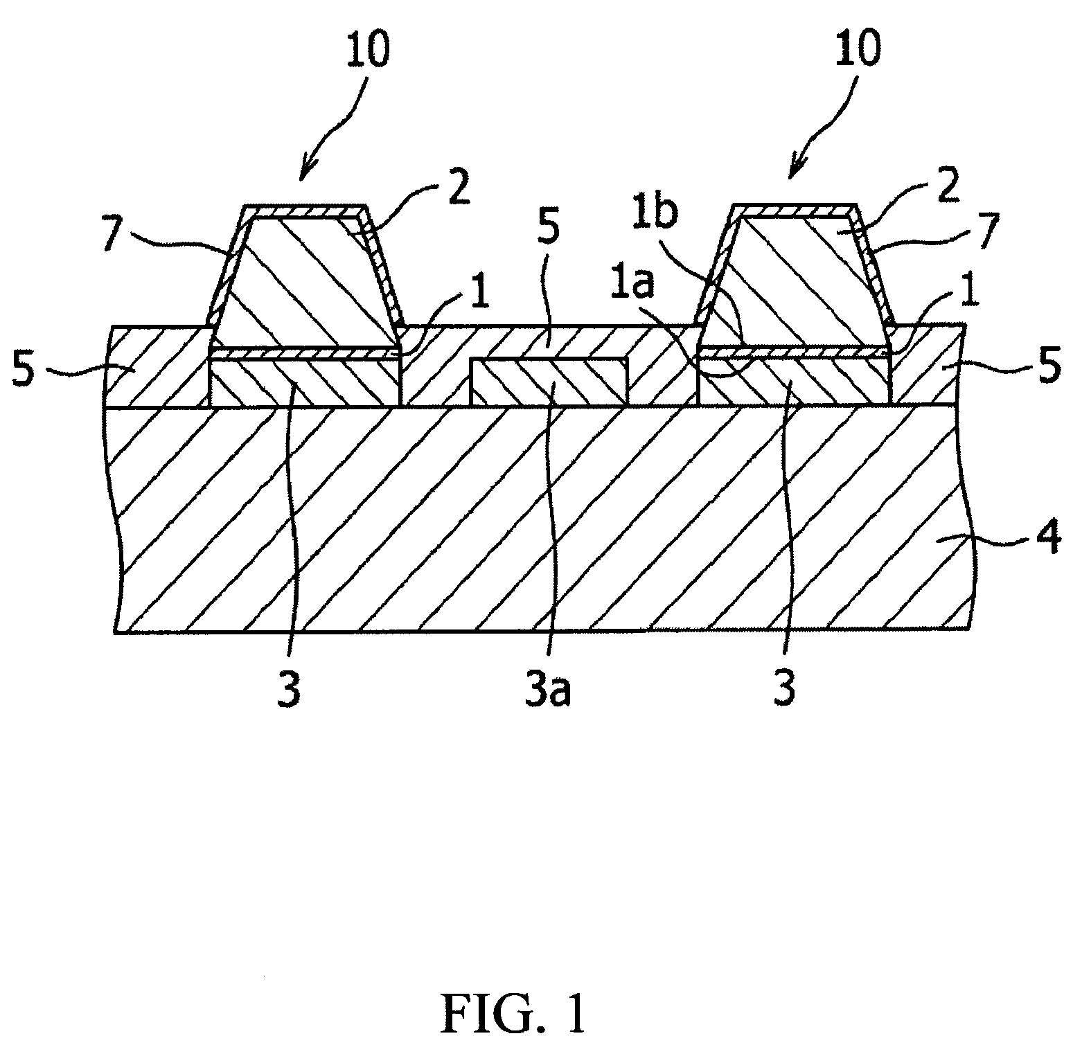
[0050]The bump 2 is formed in the same manner as in the first embodiment and the tin metal layer 1 is etched, so as to form the interconnection element 10 in which the wiring layer 3a is held as a supporting member (FIG. 5B). Thermosetting resin 9, which turns into an insulation layer, may then be disposed on a portion in which no bump structure 10 is formed (FIG. 5C). The assembly may be positioned on a substrate 44 so that the position of the bump is aligned with the position of the metal portion and with the interconnection element 10 facing the substrate 44, the entire assembly is pressurized and heated, thereby integrating the assembly and the substrate 44 being integrated (FIG. 5D). An etching resist 11 for forming the pad 3 into a predetermined pattern from the wiring layer 3a is formed on the wiring layer 3a. Using the etching resist 11, etching may be carried out, so that the pad 3 is patterned from the wiring layer 3a. A solder resist 12 is formed on a face on which the pa...

fourth embodiment

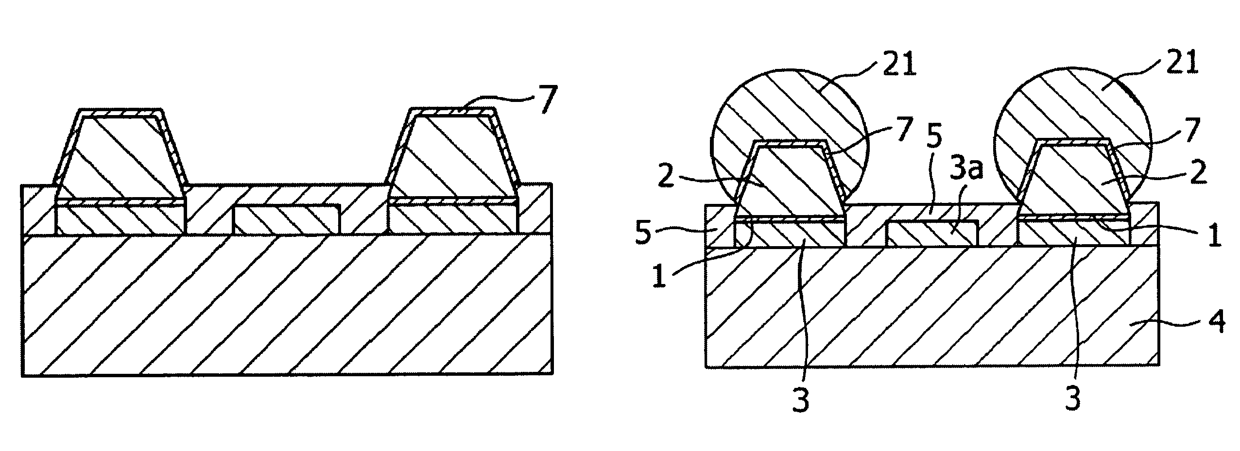
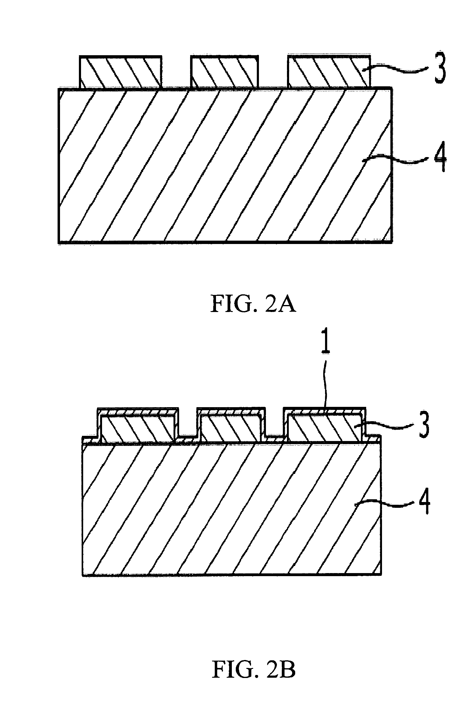
[0051]FIGS. 6A-6F, the interconnection element, show the method steps as to how the interconnection element is created and connected to an external circuit chip or the like. The interconnection element includes bump structure 10 (FIG. 6B), which includes metal bumps 2, a low melting point metal layer, such as tin layer 1, and a wiring layer 3a that is capable of providing interconnection to another electronic element or the like. The wiring layer 3a may be held by a charged encapsulant, such as a resin portion 14, which acts as an insulating portion or layer (FIG. 6D). According to this embodiment, the assembly in which the wiring layer 3a, the tin metal layer 1 and the copper foil 2a are stacked is prepared, and the etching resist 6 is disposed on the wiring layer 3a (FIG. 6A). Following the pattern of the etching resist 6, the copper foil 2a may be etched so as to form the bump 2. With the bump 2 used as a mask, the tin metal layer 1 is etched so as to obtain the interconnection e...


PUM

PropertyMeasurementUnit
melting pointaaaaaaaaaa
diameteraaaaaaaaaa
diameteraaaaaaaaaa

Abstract

An interconnection element and method for making same is disclosed. The interconnection element may include a plurality of metal conductors, a plurality of solid metal bumps and a low melting point (LMP) metal layer. The solid metal bumps overly and project in a first direction away from respective ones of the conductors. Each bump has at least one edge bounding the bump in at least a second direction transverse to the first direction. The low melting point (LMP) metal layer has a first face joined to the respective ones of the conductors and bounded in the second direction by at least one edge and a second face joined to the bumps. The edges of the bumps and the LMP layer are aligned in the first direction, and the LMP metal layer has a melting temperature substantially lower than the conductors.

Description

[0001]The embodiments disclosed herein relate to an interconnection element to methods or processes for forming such interconnection elements. More particularly, the present embodiments relate to an interconnection element used for mounting electronic circuit components such as integrated circuit chips (“IC”) for use in electronic apparatuses and to a method or process for forming such an interconnection element.BACKGROUND OF THE INVENTION[0002]It is well known in the art to use land grid array (“LGA”) type connection as a method for connecting a semiconductor chip having a plurality of connecting terminals to a printed wiring board (“PWB”) or a circuit panel, such as a printed circuit board (“PCB”), when it is desired to utilize use bumps in order to increase the mounting density of electronic circuitry. Bumps are normally formed on one face of the chip for electrical connection with the PWB. If an intermediate board, such as an interposer or a substrate is loaded with an IC so as ...

Claims


Application Information

Patent Timeline
Patent Type & Authority Patents(United States)
IPC IPC(8): H05K1/11
CPCH05K3/4007H05K3/4614H01R43/0256H01L2224/13609H05K1/185H05K3/06H05K3/4015H05K2201/0355H05K2201/0361H05K2201/10674H05K2203/0384H05K2203/0542H01L2924/01019H01L2924/01322H01L2224/05571H01L2224/05573H01L2924/00014H01L2224/06131H01L2224/05599
Inventor ENDO, KIMITAKA
Owner INVENSAS CORP
Why Eureka
Try Eureka