Laminated ceramic electronic component

a technology of laminated ceramic and electronic components, applied in the direction of fixed capacitors, fixed capacitor details, capacitors, etc., can solve the problems of reducing the variations in the properties of laminated ceramic capacitors, the fixation strength of the plating film to the ceramic element assembly is relatively low, and the inner ends of the thick film portion are blurred or indistinguishable, so as to prevent the variation of properties such as insulation resistance.

Active Publication Date: 2012-11-06
MURATA MFG CO LTD
View PDF24 Cites 6 Cited by
  • Summary
  • Abstract
  • Description
  • Claims
  • Application Information

AI Technical Summary

Benefits of technology

[0010]To overcome the problems described above, preferred embodiments of the invention provide a laminated ceramic electronic component that includes a relatively thick film portion provided at an internal electrode portion exposed at the outer surface of a ceramic element assembly, in which variations in properties, such as insulation resistance, are prevented.
[0011]Other preferred embodiments of the present invention provide a laminated ceramic electronic component in which external electrodes are formed on the front surface of a ceramic element assembly by plating, which is suitable for a reduction in size, and which has a relatively thick film portion at a portion at which internal electrodes are exposed at the outer surface of the ceramic element assembly, in which variations in properties are prevented by providing a relatively thick film portion on the internal electrodes.

Problems solved by technology

In contrast, there has been a problem with the above-mentioned plating method in that the fixing strength of the plating film to the ceramic element assembly is relatively low.
When the thick film portion is provided, there have been problems in that the inner ends of the thick film portion are overlapped with the ends of the internal electrodes connected to other electric potentials through a ceramic layer or insulation resistance is varies in a portion where the inner ends of the thick film portion are adjacent to the ends of the internal electrodes connected to other electric potentials.
This is caused by the fact that the inner ends of the thick film portion are blurred or indistinct when screen printing or other similar method is used to form the thick film portion.
Therefore, a reduction in the variations in the properties of the laminated ceramic capacitor has not been achieved.

Method used


Image

  • Laminated ceramic electronic component
  • Laminated ceramic electronic component
  • Laminated ceramic electronic component

Examples


Embodiment Construction

[0036]Hereinafter, preferred embodiments of the present invention will be described with reference to the drawings.

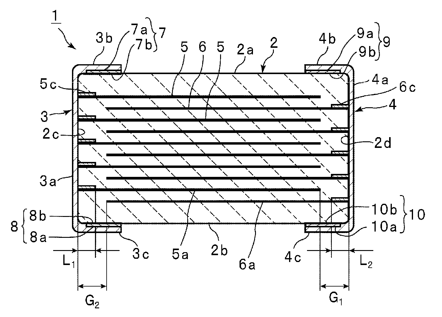
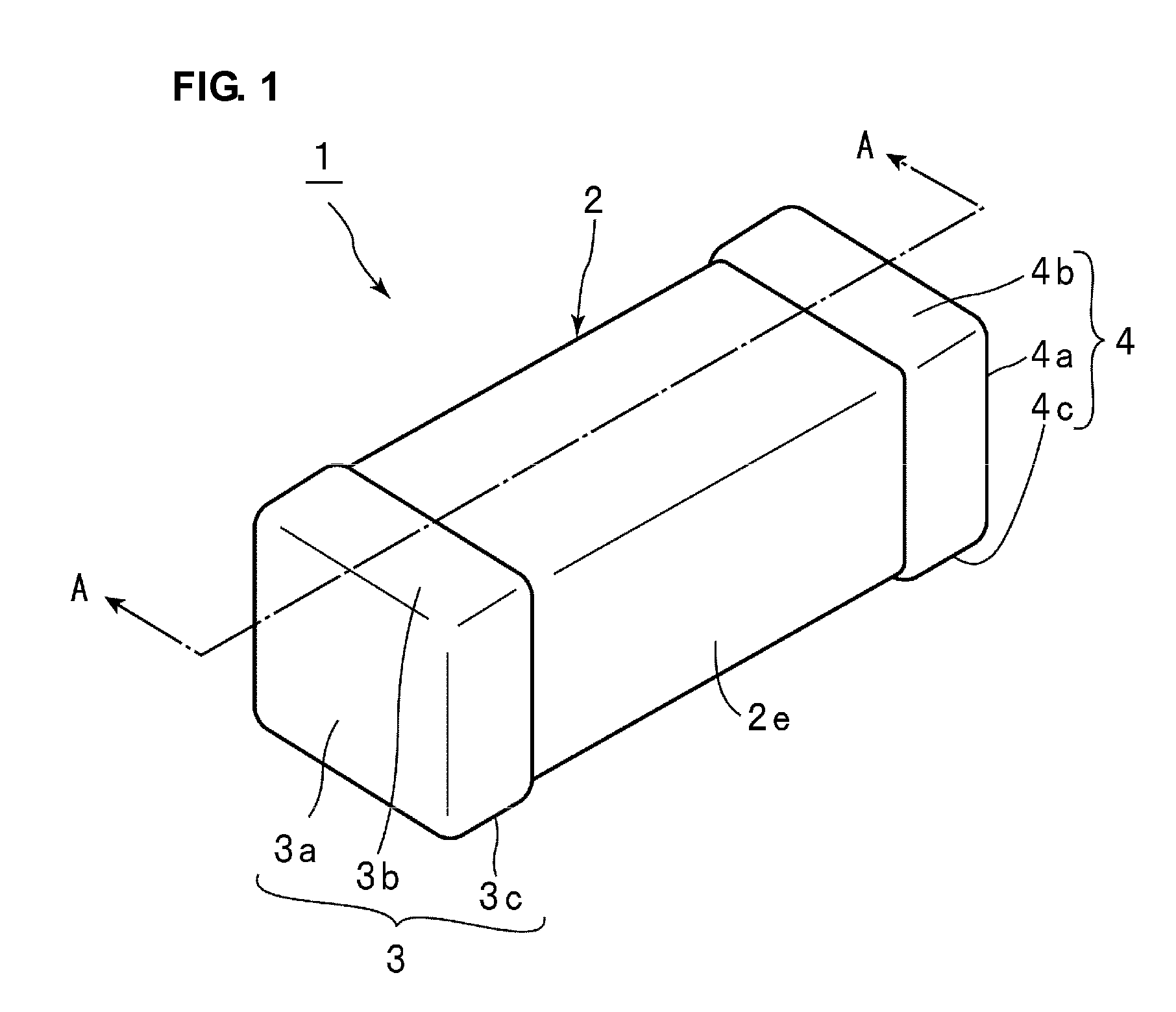
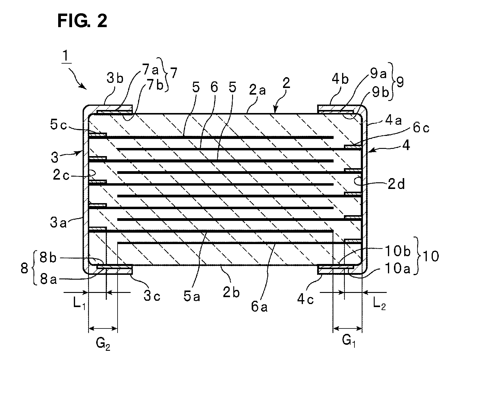
[0037]FIG. 1 is a perspective view of a laminated ceramic electronic component according to a first preferred embodiment of the present invention, and FIG. 2 is a front elevation cross sectional view thereof.

[0038]A laminated ceramic electronic component 1 of this preferred embodiment is a laminated ceramic capacitor.

[0039]The laminated ceramic electronic component 1 includes a ceramic element assembly 2 having a substantially rectangular parallelepiped shape. The ceramic element assembly 2 includes a plurality of laminated ceramic layers. The ceramic element assembly 2 has a first principal surface 2a and a second principal surface 2b that faces the first principal surface 2a. The plurality of ceramic layers are laminated in a direction in which the first and second principal surfaces 2a and 2b are connected to each other. Therefore, the direction in which the first an...


PUM

PropertyMeasurementUnit
thicknessaaaaaaaaaa
thicknessaaaaaaaaaa
thicknessaaaaaaaaaa

Abstract

A laminated ceramic electronic component includes first internal electrodes and second internal electrodes that overlap each other through ceramic layers, each of the first and second internal electrodes having first and second effective portions, first and second connecting portions, and first and second extended portions whose film thickness is greater than that of the first and second connecting portions and which are exposed at the outer surface of a ceramic element assembly. When distances from side surfaces of the ceramic assembly on which first and second external electrodes are provided to the inner edges of the first and second extended portions are defined as L1 and L2, respectively, and a distance between side surfaces and the end of the second internal electrode or the end of the first internal electrode is defined as G2 or G1, G2>L1 and G1>L2 are satisfied.

Description

BACKGROUND OF THE INVENTION[0001]1. Field of the Invention[0002]The present invention relates to a laminated ceramic electronic component, such as a laminated ceramic capacitor. More particularly, the present invention relates to a laminated ceramic electronic component in which an internal electrode extended portion includes a thick film portion whose film thickness is relatively large.[0003]2. Description of the Related Art[0004]The size of portable electronic apparatuses, such as cellular phones or digital cameras, has been increasingly reduced. Therefore, for laminated ceramic electronic components, such as a laminated ceramic capacitor, used in a portable electronic apparatus, a reduction in size and an increase in precision have been demanded. For example, in a laminated ceramic capacitor, the thickness of a ceramic layer between internal electrodes connected to different electric potentials has been reduced to be about 3 μm or less.[0005]External electrodes of the laminated c...

Claims


Application Information

Patent Timeline
Patent Type & Authority Patents(United States)
IPC IPC(8): H01G4/005H01G4/228
CPCH01G4/012H01G4/232H01G4/30
Inventor ITO, TSUYOSHISASABAYASHI, TAKEHISA
Owner MURATA MFG CO LTD
Why Eureka
Try Eureka