Piezoelectric thin film resonator and manufacturing method thereof

a thin film resonator and piezoelectric technology, applied in piezoelectric/electrostrictive transducers, device material selection, transducer types, etc., can solve the problems of inability to obtain superior resonant properties, irregularities on structural films, and unstudied planarization, etc., to achieve superior resonant properties

Inactive Publication Date: 2008-07-31
MURATA MFG CO LTD
View PDF11 Cites 6 Cited by
  • Summary
  • Abstract
  • Description
  • Claims
  • Application Information

AI Technical Summary

Benefits of technology

[0012]According to the structure described above, since the dielectric film is planarized by a plasma treatment, the orientation property of the excitation electrode formed on the dielectric film is improved, and hence the orientation property of the piezoelectric thin film formed on the excitation electrode is also improved. Since the orientation property of the piezoelectric thin film is improved, variations in resonant properties and resonant resistance can be reduced. In addition, since the orientation property of the excitation electrode is improved, a piezoelectric thin film resonator having superior resistance against electric power can be formed.
[0013]In addition, when a plurality of piezoelectric thin film resonators is simultaneously formed using a wafer, the thickness of the structural film of each resonator can be controlled on the order of nanometers. Accordingly, since variation in resonant frequency in the wafer surface and the resonant properties can be controlled with high accuracy, the yield can be increased, and hence the manufacturing cost can be reduced.
[0016]According to the above structure, since the dielectric film is an amorphous film, planarization can be easily performed by a plasma treatment.
[0019]Since the dielectric film is planarized in the above third step, the orientation property of the excitation electrode formed on the dielectric film is improved, and the orientation property of the piezoelectric thin film formed on the excitation electrode is also improved. Since the orientation property of the piezoelectric thin film is improved, a piezoelectric thin film resonator having superior resonant properties can be manufactured.
[0027]According to the piezoelectric thin film resonator and the manufacturing method thereof, by uniformly planarizing the structural film, a resonator having superior resonant properties can be obtained.

Problems solved by technology

Heretofore, planarization has not been studied for an air-bridge type piezoelectric thin film resonator.
Hence, irregularities are formed on the structural film which is to be polished.
Accordingly, even when the structural film on the sacrifice layer is polished, film-thickness distribution is generated, and as a result, superior resonant properties cannot be obtained.
In order to avoid this problem, a method may be used in which after a burying material is buried in concave portions, planarization is performed by CMP, and the burying material is then removed; however, in this case, the manufacturing process becomes complicated, and hence the manufacturing cost is increased.
In addition, when a plurality of piezoelectric thin film resonators is simultaneously formed using a wafer, it is difficult to uniformly polish structural films of individual resonators in the wafer on the order of nanometers in thickness.
When the thicknesses of the structural films vary within a wafer, the yield may be decreased, or the number of steps, such as frequency adjustment, may be increased, and as a result, the manufacturing cost is increased.

Method used


Image

  • Piezoelectric thin film resonator and manufacturing method thereof
  • Piezoelectric thin film resonator and manufacturing method thereof
  • Piezoelectric thin film resonator and manufacturing method thereof

Examples


Embodiment Construction

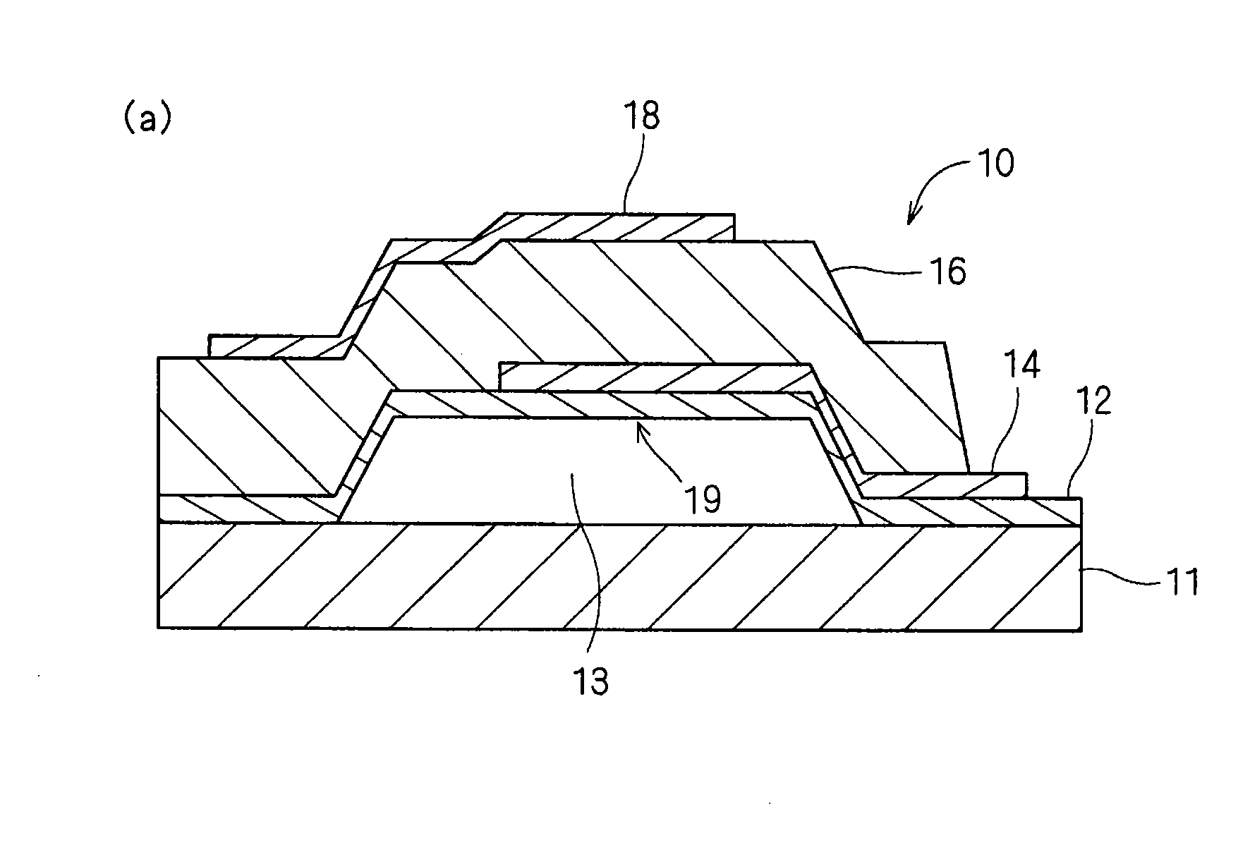
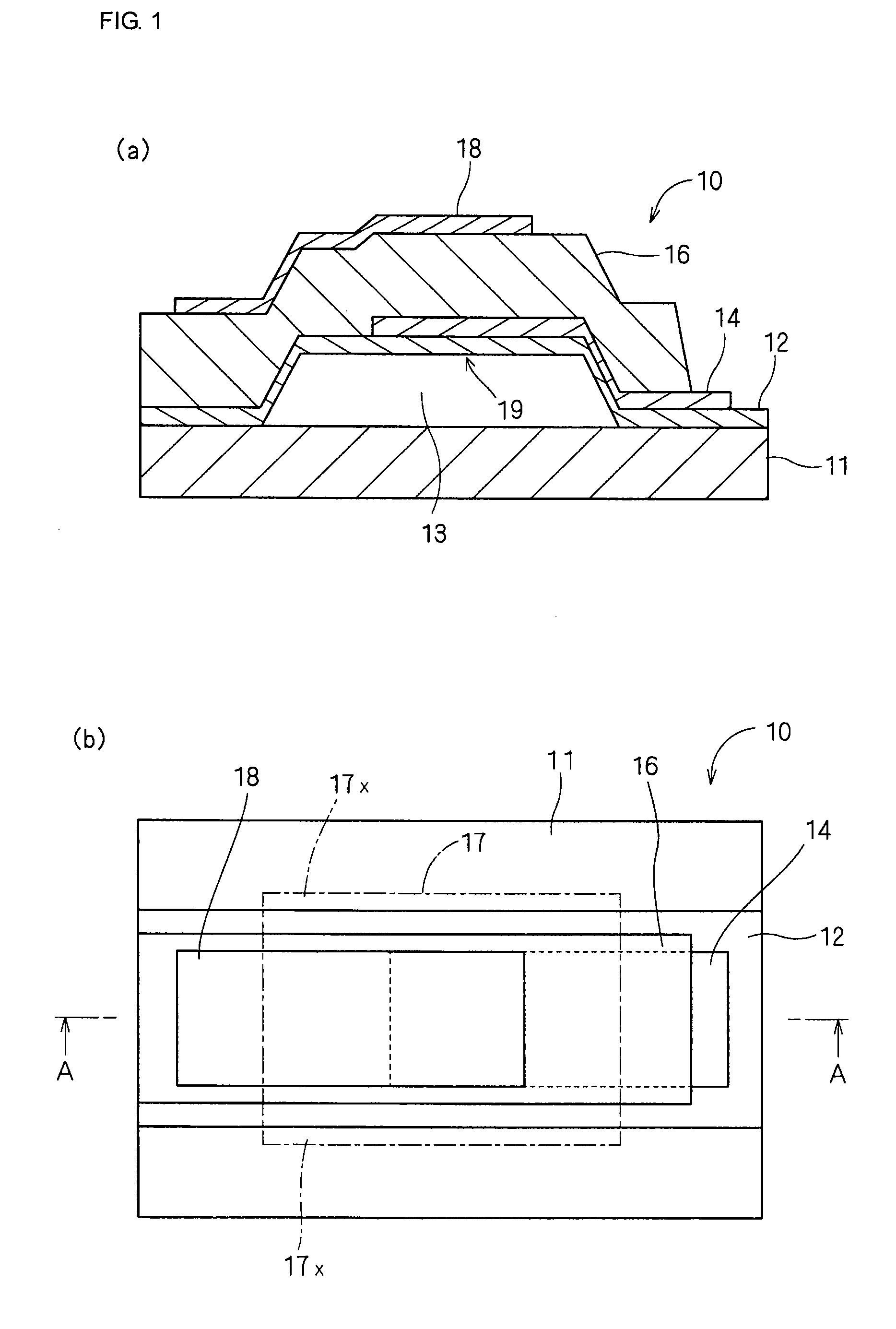
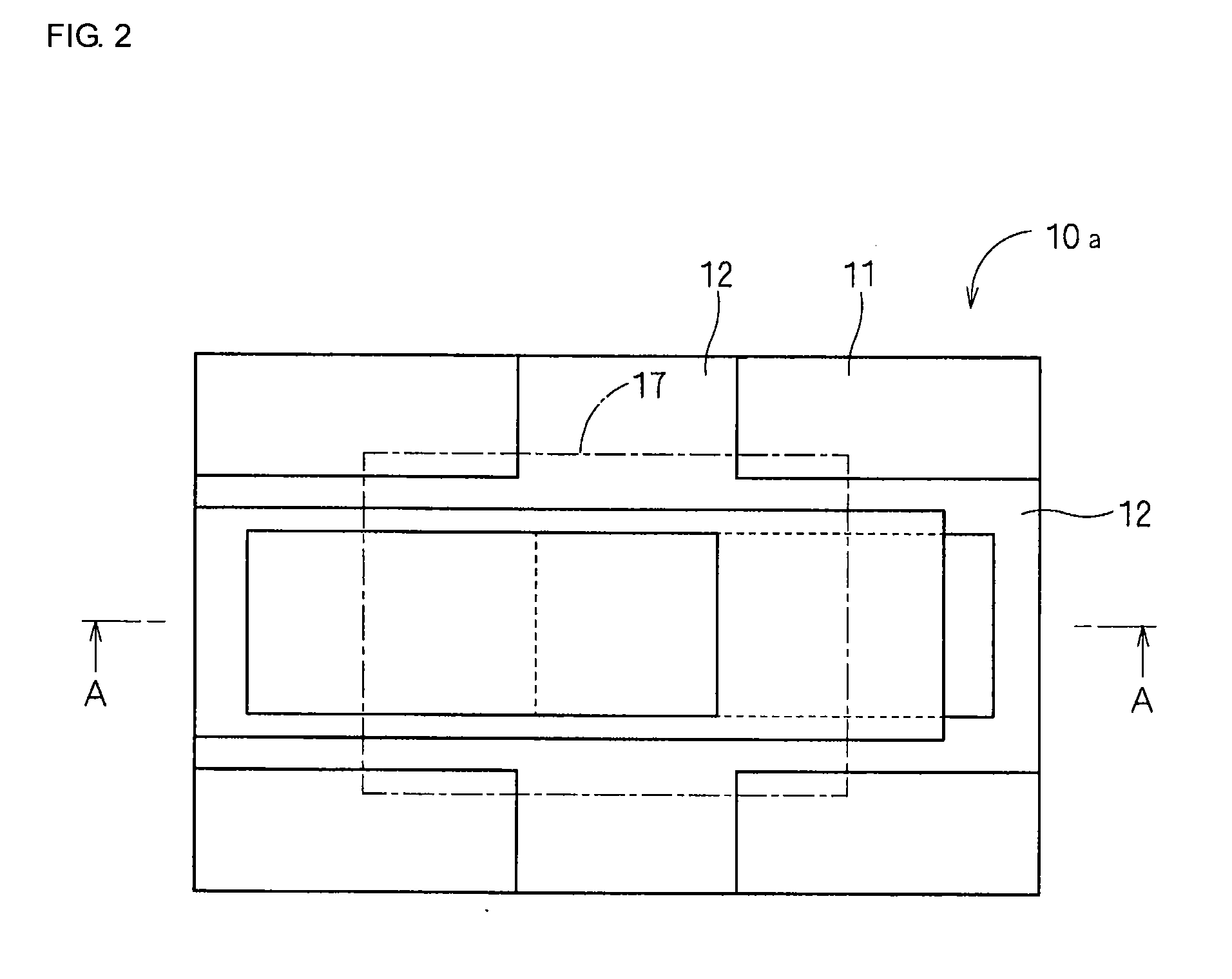
[0039]Hereinafter, examples will be described as embodiments according to the present invention with reference to FIG. 1. FIG. 1(a) is a cross-sectional view taken along the line A-A in FIG. 1(b), and FIG. 1(b) is a plan view.

[0040]As schematically shown in FIG. 1, a piezoelectric thin film resonator 10 is formed of a substrate 11 and a thin film member (membrane) provided thereon, the thin film member including a dielectric film 12, a lower electrode 14, a piezoelectric thin film 16, and an upper electrode 18. An airspace layer 13 (see FIG. 1(a)) is formed between the substrate 11 and the dielectric film 12. The dielectric film 12 includes support portions supported by the substrate 11 and a floating portion floating over the substrate 11. On the floating portion of the dielectric film 12 at a position opposite to the airspace layer 13, a vibration portion 19 floating over the substrate 11 is formed in a region in which the electrodes 14 and 18 are overlapped with each other. The v...


PUM

PropertyMeasurementUnit
thicknessaaaaaaaaaa
surface roughness Raaaaaaaaaaa

Abstract

A piezoelectric thin film resonator which can reduce variations in resonant frequency and resonant resistance by uniformly planarizing a structural film, and a method of manufacturing the piezoelectric thin film resonator. The piezoelectric thin film resonator has a substrate having at least one flat major surface; a dielectric film having two support portions supported by the major surface of the substrate and a floating portion which is connected to the support portions and which is disposed over the major surface of the substrate with an airspace layer provided therebetween; and a vibration portion which is formed of a pair of electrodes and a piezoelectric thin film provided therebetween and which is provided on the floating portion of the dielectric film at a side opposite to the airspace layer. A surface of the dielectric film at a side opposite to the substrate is planarized by a plasma treatment using an inert gas or a gas containing an element forming a dielectric film.

Description

CROSS REFERENCE TO RELATED APPLICATIONS[0001]The present application is a divisional of application Ser. No. 11 / 714,870, filed Mar. 6, 2007, which is a continuation of International Application No. PCT / JP2005 / 022300, filed Dec. 5, 2005, claiming priority to Japanese Patent Application No. JP2004-373761, filed Dec. 24, 2004, the entire contents of each of these applications being incorporated herein by reference in their entirety.FIELD OF THE INVENTION[0002]The present invention relates to a piezoelectric thin film resonator and a manufacturing method thereof.BACKGROUND OF THE INVENTION[0003]In a so-called air-bridge type piezoelectric thin film resonator, in order to acoustically separate a vibration portion, which is formed of a pair of excitation electrodes facing each other and a piezoelectric thin film provided therebetween, from a substrate, the structure is formed in which a thin film member (membrane) partly floats over the substrate with an airspace layer provided there betw...

Claims


Application Information

Patent Timeline
Patent Type & Authority Applications(United States)
IPC IPC(8): H01L41/22H01L41/09H01L41/18H01L41/332H01L41/338H01L41/39H03H3/02H03H9/17
CPCH03H3/04H03H9/173H03H2003/021Y10T29/49005Y10T29/49798Y10T29/42Y10T29/49155Y10T29/49128
Inventor FUJII, HIDETOSHIKUBO, RYUICHI
Owner MURATA MFG CO LTD
Why Eureka
Try Eureka