Print head and image forming device having the same

a technology of image forming device and print head, which is applied in the field of print head, can solve the problems of uneven exposure along the photoreceptor surface line, further improvement of calibration accuracy, and differences in light emission amount with respect to constant current, and achieves improved image quality and image quality. the effect of image forming device and higher performan

Active Publication Date: 2020-04-28
KONICA MINOLTA INC
View PDF17 Cites 0 Cited by
  • Summary
  • Abstract
  • Description
  • Claims
  • Application Information

AI Technical Summary

Benefits of technology

[0006]In recent years, demand for miniaturization and higher image quality with respect to image forming devices has further increased. Accordingly, higher performance is sought for print heads of the light-emitting-element-array type. As a means of meeting such demands, use of organic light-emitting diodes (OLEDs) as a light source is being considered. In comparison with LEDs, OLEDs are advantageous in having a low black level, high color expression, and low power consumption, and can easily be made compact, thin, and light. On the other hand, variation in structure and (initial) properties between light emitting elements is greater for OLEDs than LEDs. Further, OLEDs have a faster rate of light emission amount decrease (light amount deterioration) as cumulative total light emission time increases than LEDs. Speed of light amount deterioration varies depending on light emission amount and light emitting element temperature, and therefore differences occur in light amount deterioration due to differences in usage history even between light emitting elements having the same initial properties. Accordingly, particularly when using OLEDs as light sources, it is desirable that print heads, during usage, periodically repeat calibration of light emission amounts of light receiving elements.
[0008]An object of the present invention is to solve the problems described above, and more particularly to provide a print head capable of further improving accuracy of calibration of light emission amounts by using a light receiving element, regardless of individual differences between light emitting elements.

Problems solved by technology

On the other hand, light-emitting-element-array types of print head may have variations (individual differences) in structure and (initial) properties between light emitting elements, which may cause differences in light emission amounts with respect to a constant current.
In other words, uneven amounts of light may be emitted, and there is therefore a risk of uneven exposure along a line of the photoreceptor surface.
However, there is a problem with light-emitting-element-array types of print head in that further improvement in accuracy of calibration of light emission amounts by using a light receiving element, i.e., further reduction of acceptable error between the estimated and target values of light emission amounts, is difficult for the following reasons.
These differences impart variation to values measured by the light receiving element even if light emission amounts are uniform between the light emitting elements, and impart error to estimated light emission amounts from the light emitting elements estimated from the measured values.
Such errors in the gain destabilize feedback control of light emission amounts.
In particular, when the target value of light emission amount is large, there is a risk that actual light emission amounts are saturated to an acceptable upper limit, and when the target value is small, there is a risk that the amounts of light reaching the light receiving element falls below an acceptable lower limit.
In either case the light receiving element is unable to accurately measure the light amounts.

Method used


Image

  • Print head and image forming device having the same
  • Print head and image forming device having the same
  • Print head and image forming device having the same

Examples


Embodiment Construction

[0018]The following is a description of one or more embodiments of the present invention with reference to the drawings. However, the scope of the invention is not limited to the embodiments described.

[Image Forming Device Appearance]

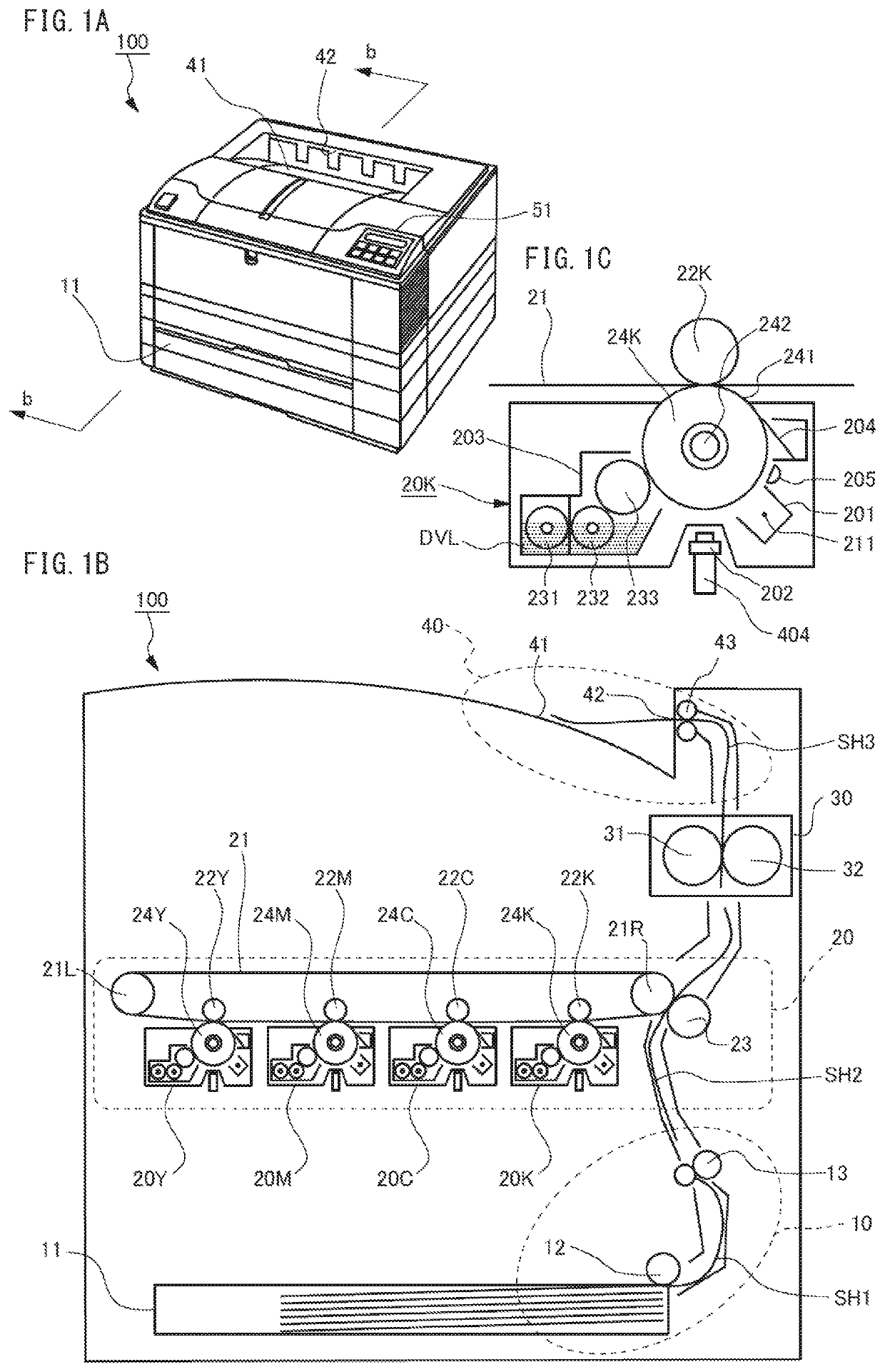
[0019]FIG. 1A is a perspective view illustrating appearance of an image forming device 100 pertaining to an embodiment of the present invention. The image forming device 100 is a printer. A discharge tray 41 is provided on a top surface of a casing of the image forming device 100, and stores sheets discharged from a discharge opening 42 towards a rear of the image forming device 100. An operation panel 51 is embedded forward of the discharge tray 41. A paper feed cassette 11 is attached to a bottom portion of the printer 100 in a way that allows the paper feed cassette 11 to be pulled out.

[Internal Configuration of Printer]

[0020]FIG. 1B is a schematic cross section of the printer 100 taken along the straight line b-b indicated in FIG. 1A. The printer 10...


PUM

PropertyMeasurementUnit
diameteraaaaaaaaaa
charge distributionaaaaaaaaaa
timeaaaaaaaaaa

Abstract

A print head for writing data onto a photoreceptor, including a light source panel of light emitting elements arranged in a matrix, optical systems arranged in a matching matrix, light receiving elements, and a corrector. The optical systems each include at least a light-source-side lens and an image-side lens, and focus light from the light emitting elements onto different regions of the photoreceptor. The light receiving elements each include a light receiving surface disposed in a leaked light region and detect light incident on the light receiving surface. The leaked light region is in a gap between the light-source-side lens and the image-side lens of each of the optical systems occupied by optical paths of light transmitted through the light-source-side lenses but not incident on the image-side lenses. The corrector corrects amounts of light to be emitted from the light emitting elements based on the light detected.

Description

[0001]This application claims priority to Japanese Patent Application No. 2017-174273, filed Sep. 11, 2017, the contents of which are hereby incorporated herein by reference in their entirety.BACKGROUNDTechnical Field[0002]The present disclosure relates to electrophotographic image forming devices, and in particular to print heads that expose photoreceptors to light modulated according to image data.Description of the Related Art[0003]A print head (PH) exposes a photoreceptor surface to light in an electrophotographic image forming device such as a printer or copying machine, or in other words irradiates a charged region of a photoreceptor surface with light modulated according to image data to form a charge distribution corresponding to variation in light irradiation, i.e., an electrostatic latent image. The photoreceptor covers an outer circumferential surface of a rotating body such as a drum or a belt rotatably supported in the image forming device. The print head exposes the ph...

Claims


Application Information

Patent Timeline
Patent Type & Authority Patents(United States)
IPC IPC(8): G03G15/043G03G15/04G03G15/32G02B5/00
CPCG03G15/04036G03G15/04054G03G15/043G03G15/326G02B5/005G03G15/0409
Inventor UEMURA, TAKAKIOBAYASHI, MAKOTOIIJIMA, MASAYUKI
Owner KONICA MINOLTA INC
Why Eureka
Try Eureka