Switching element and application of the same

a technology of switching elements and elements, applied in the field of switching elements, can solve the problems of inability to produce inability to exhibit expected performance of circuits and memory devices fabricated by integrating switching elements, and inability to form uniform plurality of such microstructures, etc., to achieve the effect of reducing the property fluctuation of individual switching elements of the invention, reducing the resistance between electrodes, and reducing the expected performan

Inactive Publication Date: 2012-11-27
NAT INST FOR MATERIALS SCI
View PDF12 Cites 1 Cited by
  • Summary
  • Abstract
  • Description
  • Claims
  • Application Information

AI Technical Summary

Benefits of technology

[0016]The space between the ionic conductor part of the first electrode and the second electrode is preferably at most 80 nm, from the viewpoint of preventing resistance fluctuation and preventing operation failure such as delay or electric connection breakage in use in electronic circuits, etc.; and its lowermost limit is preferably 3 nm, more preferably 5 nm, even more preferably 10 nm.
[0022]In that manner, a carrier can be generated in the photoresponsive film through photoirradiation and the deposition of metal from the ionic conductor can be accelerated through the carrier supply, and therefore in case where practicable voltage application and operating time are estimated, the distance between the first electrode and the second electrode can be broadened as compared with a case where an ordinary insulation film is used. As a result, when worked with accuracy on the same level, the property fluctuation of the individual switching elements of the invention can be reduced as compared with that of the structure comprising an ordinary insulation film, and the circuit device and the memory device with the switching elements of the invention integrated therein can exhibit the expected performance.
[0023]When used in a memory device, the distance between the first electrode and the second electrode is broad as compared with a case where an ordinary insulation film is used, and therefore, even though the condition of the deposited metal may change through voltage application between electrodes in reading out, the condition of the switching element does not unintentionally change from the connected to the non-connected condition or from the non-connected condition to the connected condition in long-term use.
[0024]Further, in use as a part of reconfigurable wiring in an electronic circuit, the metal deposition is accelerated through supply of the carrier generated from the photoresponsive film by photoirradiation, and therefore, the two electrodes can be rapidly and firmly connected to each other with the result that the resistance between the electrodes can be reduced and the wiring characteristic on the same level as that in ordinary wiring can be expected.

Problems solved by technology

However, it is difficult to form uniformly a plurality of such microstructures on an atomic order, and fluctuation in the distance between the two electrodes is inevitable.
However, as mentioned above, the distance between the two electrodes fluctuates, and therefore, for example, the time for electric connection between the two electrodes under the condition of predetermined voltage application thereto may also fluctuate, and the circuits and the memory devices fabricated by integrating the switching elements could not exhibit the expected performance.

Method used


Image

  • Switching element and application of the same
  • Switching element and application of the same
  • Switching element and application of the same

Examples


first embodiment

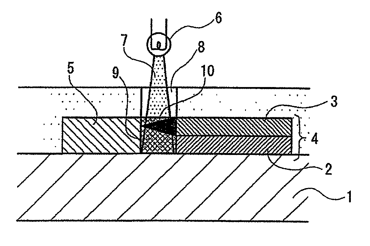
[0032]FIG. 1 is a cross-sectional view schematically showing a switching element (photoassisted switching element) of the first embodiment of the invention. As illustrated in the drawing, the switching element comprises a first electrode 4 and a second electrode 5 provided on an insulating substrate 1, in which these electrodes are disposed in a line with interval therebetween on the insulating substrate 1.

[0033]The first electrode 4 is composed of a first electrode electric conductor part 2 and a first electrode ionic conductor part 3, and the first electrode ionic conductor part 3 is formed, as laminated on the first electrode electric conductor part 2.

[0034]Between the first electrode 4 and the second electrode 5, disposed is a photoresponsive film 9 so as to fill up the space between the electrodes, more concretely, so as to fill up the space between the first electrode ionic conductor part 3 of the first electrode 4 and the second electrode 5. The photoresponsive film 9 is so d...

second embodiment

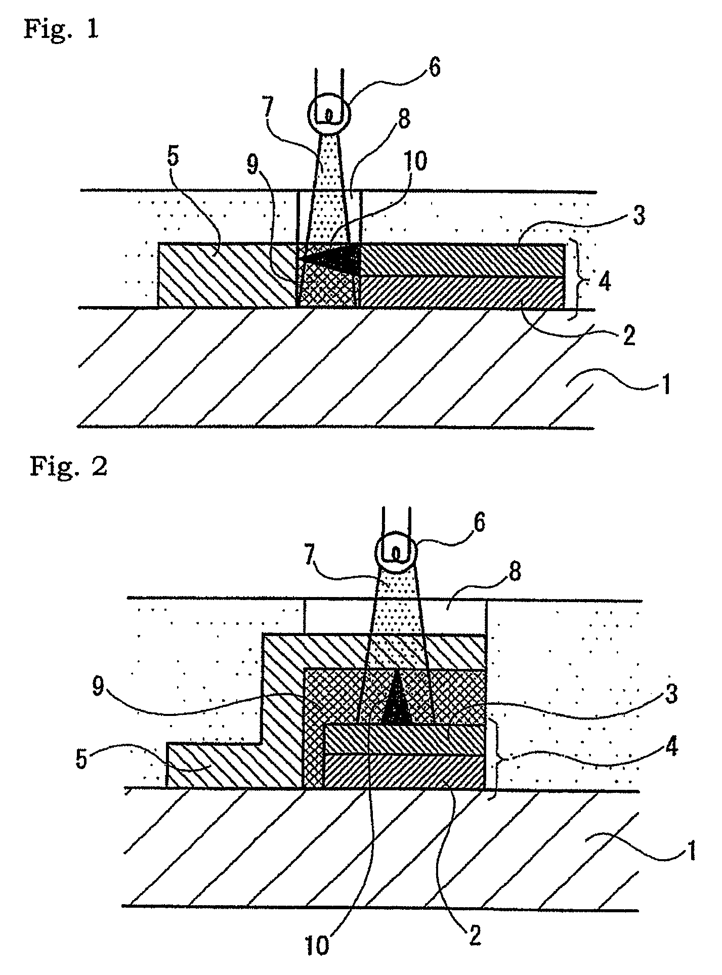
[0044]FIG. 2 is a cross-sectional view schematically showing a switching element (photoassisted switching element) of the second embodiment of the invention. In this embodiment, the constitutive components common to those in the first embodiment are given the same reference numerals or signs.

[0045]As illustrated in the figure, the switching element comprises a first electrode 4 and a second electrode 5 formed on an insulating substrate 1. The first electrode 4 is composed of a first electrode electric conductor part 2 and a first electrode ionic conductor part 3, and the first electrode ionic conductor part 3 is formed, as laminated on the first electrode electric conductor part 2. The second electrode 5 is composed of a transparent electric conductor.

[0046]Between the first electrode 4 and the second electrode 5, disposed is a photoresponsive film 9 so as to fill up the space between the electrodes; and in the region of the light-receiving part of the photoresponsive film 9, the fi...

third embodiment

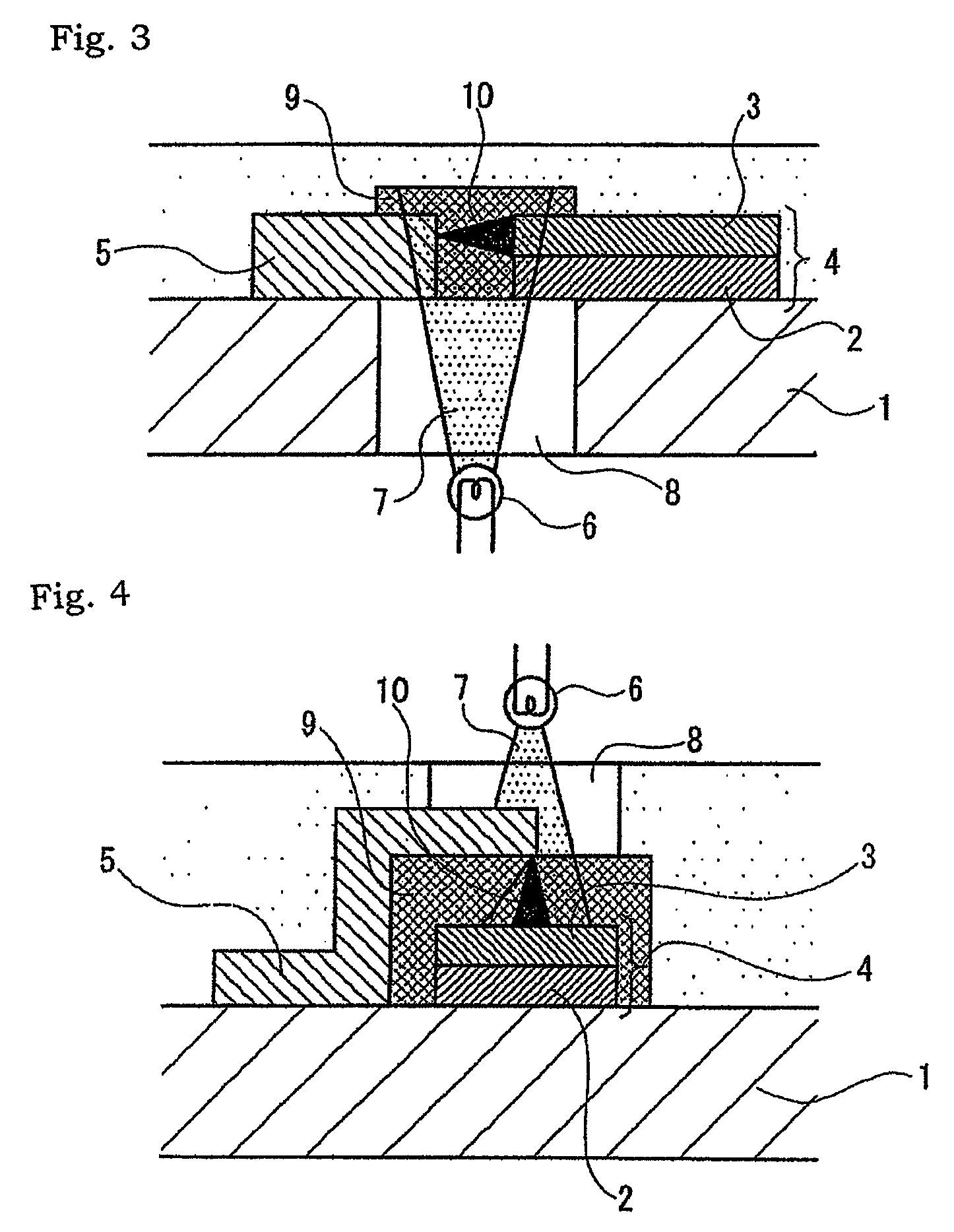
[0057]FIG. 3 is a cross-sectional view schematically showing a switching element (photoassisted switching element) of the third embodiment of the invention. In this embodiment, the constitutive components common to those in the first embodiment are given the same reference numerals or signs.

[0058]As illustrated in the figure, the switching element comprises a first electrode 4 and a second electrode 5 formed on an insulating substrate 1, in which these electrodes are disposed in a line with interval therebetween on the insulating substrate 1.

[0059]The first electrode 4 is composed of a first electrode electric conductor part 2 and a first electrode ionic conductor part 3, and the first electrode ionic conductor part 3 is formed, as laminated on the first electrode electric conductor part 2.

[0060]Between the first electrode 4 and the second electrode 5, disposed is a photoresponsive film 9 so as to fill up the space between the electrodes, more concretely, so as to fill up the space ...


PUM


Abstract

A micro-switching element provided with a first electrode 4 containing an ionic conductor and a second electrode 5 composed of an electric conductor, wherein the first electrode 4 and the second electrode 5 are physically and electrically connected to each other through deposition of a metal ion from the ionic conductor, and wherein a photoresponsive film 9 that receives light to generate a carrier is disposed between the first electrode 4 and the second electrode 5 to fill up the space between the electrodes. Accordingly, a micro-switching element is provided of which the characteristic fluctuation is small and which hardly produces a problem of operation failure.

Description

TECHNICAL FIELD[0001]The present invention relates to a switching element and application of the same.BACKGROUND ART[0002]Heretofore, as micro-switching elements, proposed are those provided with a first electrode including an ionic conductor and a second electrode composed of an electric conductor (see Patent Document 1 (JP-A 2002-76325 (paragraphs [0011] to [0019]), Patent Document 2 (JP-A 2002-141494 (paragraphs [0030] to [0089]), Patent Document 3 (JP-A 2002-334989 (paragraphs [0017] to [0059]), Patent Document 4 (JP-A 2003-094227)). For example, Patent Reference 1 discloses a switching element in which the metal ion in the first electrode is deposited from the surface of the first electrode toward the second electrode by the tunneling current between the first electrode and the second electrode generated through voltage application between the electrodes whereby the electrodes are physically and electrically connected to each other by the deposited metal, and in which the physi...

Claims


Application Information

Patent Timeline
Patent Type & Authority Patents(United States)
IPC IPC(8): G11C13/00
CPCH01L51/4206H01L45/14H01L45/1213H01L45/1226H01L45/1233H01L45/1266H01L45/085H01L51/0053H01L51/0591Y02E10/549H10N70/245H10N70/257H10N70/823H10N70/8416H10N70/881H10N70/826H10K85/621H10K10/50H10K30/451
Inventor HASEGAWA, TSUYOSHIAONO, MASAKAZUYANO, FUMIKOTERABE, KAZUYATSURUOKA, TORUEBIHARA, TOMOKOOGAWA, TAKUJITANAKA, HIROFUMIHINO, TAKAMI
Owner NAT INST FOR MATERIALS SCI
Why Eureka
Try Eureka