

Anti-static part and its manufacturing method
a technology of anti-static parts and manufacturing methods, applied in the direction of spark plugs, emergency protective arrangements for limiting excess voltage/current, nuclear engineering, etc., can solve the problems of large repulsive force, degrade signal quality, breakage of electronic components, etc., to achieve stable characteristics of suppressing electrostatic discharge, low peak voltage, and high resistance to sulfidation
- Summary
- Abstract
- Description
- Claims
- Application Information
AI Technical Summary
Benefits of technology
Problems solved by technology
Method used
Image

Examples
exemplary embodiment 1
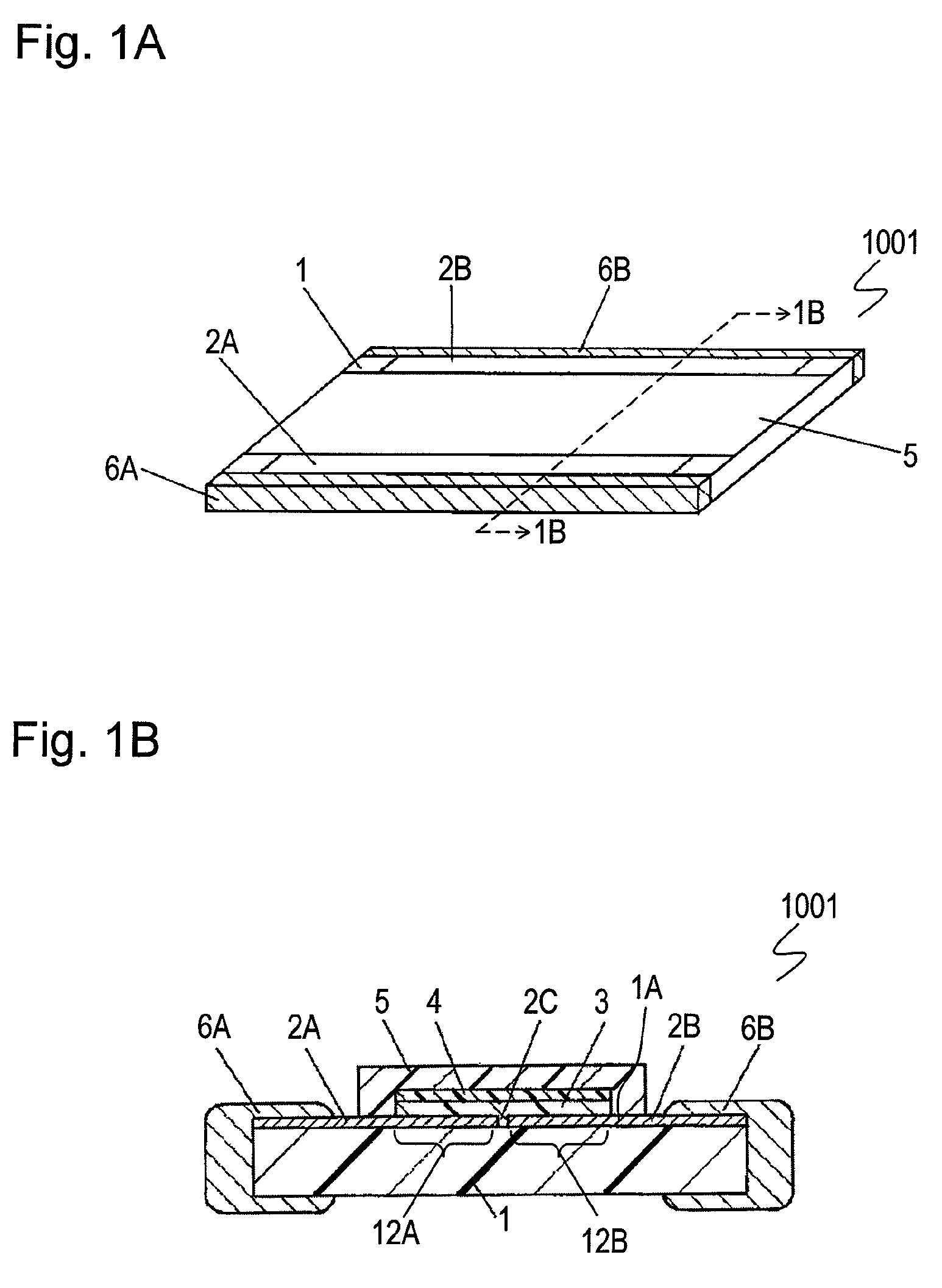
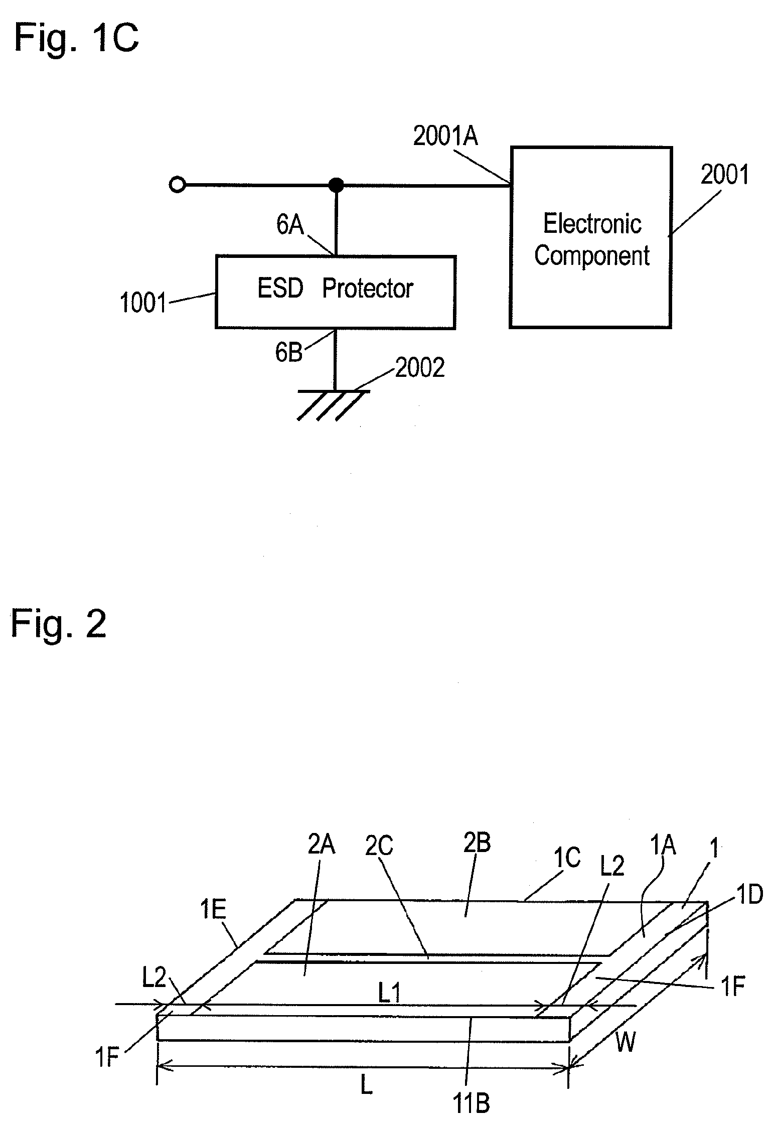
[0089]FIG. 1A is a perspective view of electrostatic discharge (ESD) protector 1001 in accordance with Exemplary Embodiment 1 of the present invention. FIG. 1B is a sectional view of ESD protector 1001 at line 1B-1B shown in FIG. 1A. Insulating substrate 1 is made of dielectric ceramic, such as alumina, having a low dielectric constant smaller than 50, preferably smaller than 10. Electrodes 2A and 2B are provided on surface (upper surface) 1A of insulating substrate 1. Electrode 2A faces electrode 2B across gap 2C having a predetermined interval. Overvoltage protective layer 3 covers portion 12A of electrode 2A, portion 12B of electrode 2B, and gap 2C. Overvoltage protective layer 3 contains insulating resin, such as silicone resin, and conductive particles, such as metal powder, dispersed in the insulating resin. Intermediate layer 4 is provided on overvoltage protective layer 3 so as to cover overvoltage protective layer 3. The intermediate layer contains insulating resin, such as...
exemplary embodiment 2
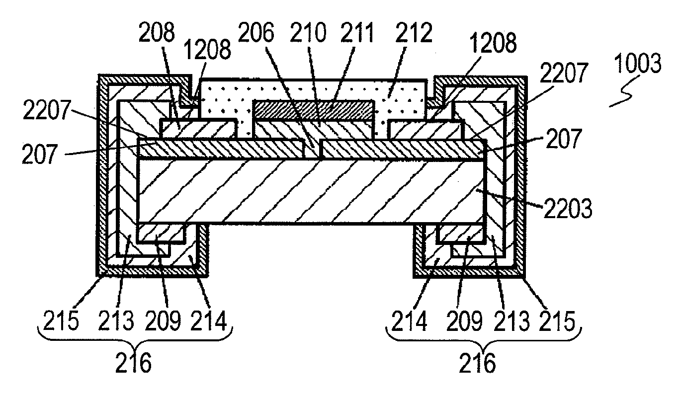
[0111]FIG. 10 is a sectional view of ESD protector 1002 in accordance with Exemplary Embodiment 2 of the present invention. FIGS. 11 to 18 are perspective views of manufacturing ESD protector 1002 for illustrating a method of manufacturing ESD protector 1002. Insulating substrate 101 is made of low-dielectric ceramic, such as alumina, having a low dielectric constant equal to or smaller than 50, preferably smaller than 10. Electrodes 102A and 102B are provided on surface (upper surface) 101A of insulating substrate 101. Electrode 102A faces electrode 102B across gap 103 having a predetermined spacing. Overvoltage protective layer 104 covers portion 112A of electrode 102A, portion 112B of electrode 102B, and gap 103. Overvoltage protective layer 104 contains insulating resin, such as silicone resin, and conductive particles, such as metal powder, dispersed in the insulating resin. Intermediate layer 105 is provided on overvoltage protective layer 104 and covers overvoltage protective...
exemplary embodiment 3
[0123]FIGS. 19A, 19C, and 19E are top views of an ESD protector according to Exemplary Embodiment 3 for illustrating a method of manufacturing the ESD protector. FIGS. 19B, 19D, and 19F are sectional views of the ESD protector at lines 19B-19B, 19D-19D, and 19F-19F shown in FIGS. 19A, 19C, and 19E, respectively.
[0124]Low-dielectric material, such as alumina, having a dielectric constant equal to or smaller than 50, preferably smaller than 10, is fired at a temperature ranging from 900 to 1600° C., thereby providing insulating substrate 203 having a sheet shape.
[0125]As shown in FIGS. 19A and 19B, plural first dividing lines 201 and plural second dividing lines 202 crossing first dividing lines 201 perpendicularly to lines 201 are defined on upper surface 203A of insulating substrate 203 having the sheet shape. First dividing lines 201 are parallel to each other. Second dividing lines 202 are parallel to each other. Dividing grooves may be formed in upper surface 203A of insulating s...
PUM
 Abstract
Description
Claims
Application Information