Resonant tunneling diode based on InGaAs/AlAs material

A resonant tunneling and diode technology, applied in diodes and other directions, can solve the problems of small electron mobility and saturation speed, and achieve the effects of reducing transit time, increasing operating frequency, and increasing peak-to-valley current ratio.

Inactive Publication Date: 2016-08-10
SUZHOU INST OF NANO TECH & NANO BIONICS CHINESE ACEDEMY OF SCI
View PDF4 Cites 4 Cited by
  • Summary
  • Abstract
  • Description
  • Claims
  • Application Information

AI Technical Summary

Problems solved by technology

However, compared with InGaAs / AlAs materials, the electron mobility and saturation velocity of Ge / Si and InAlN / GaN material systems are smaller, and only resonant tunneling diodes with lower frequency or operating speed can be fabricated.

Method used


Image

  • Resonant tunneling diode based on InGaAs/AlAs material
  • Resonant tunneling diode based on InGaAs/AlAs material
  • Resonant tunneling diode based on InGaAs/AlAs material

Examples


Embodiment Construction

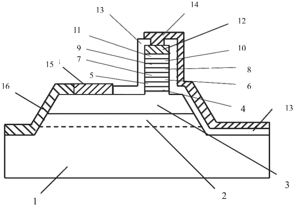
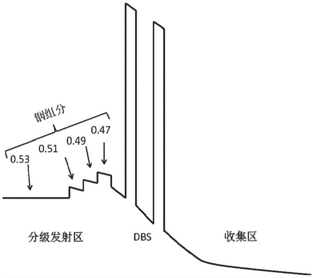
[0018] In order to realize nanoelectronic devices with extremely high frequency and working speed, the present invention proposes a resonant tunneling diode based on InGaAs / AlAs material, using n-type InP as the substrate; heavily doped InGaAs to form the emission layer and the collection area; Use the strained InGaAs layer as the quantum well and AlAs as the potential barrier to form a double barrier single potential well structure (DBS); a mesa structure formed by n-type heavily doped high In composition InGaAs is formed on the substrate and the mesa respectively Au / Pi / Ti metal electrodes.

[0019] The technical solution of the present invention will be further described below in conjunction with the accompanying drawings.

[0020] figure 1 Shown is a schematic diagram of the mesa structure of a resonant tunneling diode based on InGaAs / AlAs.

[0021] This InGaAs / AlAs-based resonant tunneling diode includes, from bottom to top:

[0022] InP substrate layer 1;

[0023] An ...


PUM


Abstract

The invention relates to the technical field of diodes, especially a resonant tunneling diode based on an InGaAs/AlAs material. InGaAs with different In components is prepared on an InP substrate layer, and a graded transmission layer structure is formed. The diode can reduce the transit time of electrons in a diode, and improves the working speed. The diode employs InxGal-xAs (x=0.8) as a potential well material, and can reduce a start voltage and a peak voltage. Non-doped InGaAs layers are respectively deposited between a transmission layer and a first barrier layer, and between a collection region and a second barrier layer, and an isolation region is formed, thereby preventing foreign matters in a heavily-doped region from diffusing towards a DBS region. According to the invention, an apparent negative differential resistance phenomenon can be observed under the room temperature, and the diode is very high in frequency and working speed. The diode can be applied to a high-speed digital circuit, a high-frequency oscillation device and the assembly of a high-quality display more effectively.

Description

technical field [0001] The invention relates to the technical field of nanometer devices, in particular to a resonance-based tunneling diode. Background technique [0002] According to Moore's Law, the electronic technology represented by silicon base has continuously reduced the feature size of devices, and has faced the physical limit, process limit and device structure limit of the device. Under these extreme conditions, nanoelectronic devices based on the quantum tunneling effect emerge as the times require. Among them, the resonant tunneling diode has a unique differential negative resistance phenomenon, so it has the remarkable characteristics of fast response speed, high operating frequency, low voltage, low power consumption, etc., especially when realizing the same function, the number of components required is large The reduced amplitude is beneficial to reduce the chip area, which makes it have broad application prospects in high-frequency oscillators and high-sp...

Claims


Application Information

Patent Timeline
Patent Type & Authority Applications(China)
IPC IPC(8): H01L29/88
Inventor 杨文献陆书龙吴渊渊谭明
Owner SUZHOU INST OF NANO TECH & NANO BIONICS CHINESE ACEDEMY OF SCI
Why Eureka
Try Eureka