Surface plasma effect based InGaAs optical detector allowing absorption enhancement

A surface plasmon and photodetector technology, applied in semiconductor devices, photovoltaic power generation, electrical components, etc., can solve the problem of carrier generation-large recombination current, increased carrier transit time, slow device response speed, etc. problems, to achieve the effects of easy processing and preparation, reduced transit time, and reduced recombination current

Active Publication Date: 2014-07-23
INST OF SEMICONDUCTORS - CHINESE ACAD OF SCI
View PDF4 Cites 15 Cited by
  • Summary
  • Abstract
  • Description
  • Claims
  • Application Information

AI Technical Summary

Problems solved by technology

[0005] In the process of realizing the present invention, the applicant found that the prior art InGaAs infrared photodetector has the following technical defects: due to the thickness of the existing detector structure absorbing layer is relatively thick, the generation and recombination current of carriers is relatively large, which becomes One of the main sources of dark current; at the same time, the thickness of the thicker absorbing layer will increase the transit time of carriers, resulting in slower response speed of the device; for the flat metal structure, it can only play a reflective role. The effect increases the propagation length of light; while the use of a one-dimensional periodic grating structure will improve the absorption enhancement to a certain extent, but it will have a strong selectivity for the polarization direction of light

Method used


Image

  • Surface plasma effect based InGaAs optical detector allowing absorption enhancement
  • Surface plasma effect based InGaAs optical detector allowing absorption enhancement
  • Surface plasma effect based InGaAs optical detector allowing absorption enhancement

Examples


Embodiment Construction

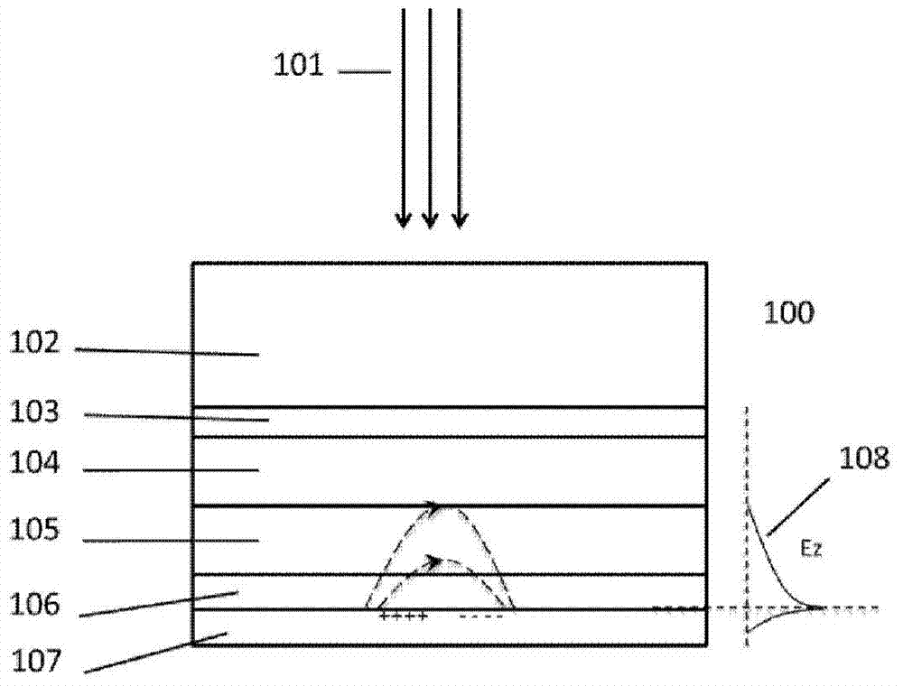
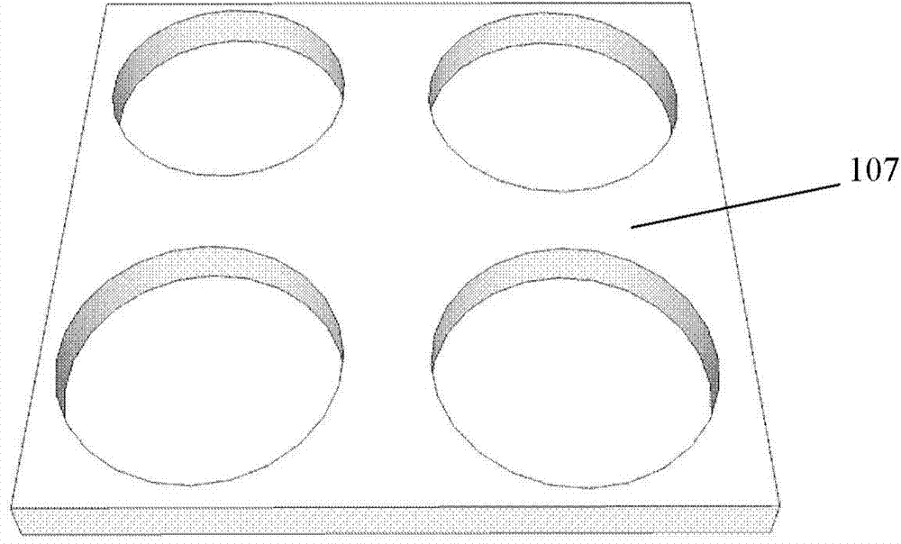
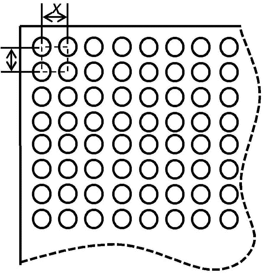
[0027] In order to make the object, technical solution and advantages of the present invention clearer, the present invention will be described in further detail below in conjunction with specific embodiments and with reference to the accompanying drawings. It should be noted that, in the drawings or descriptions of the specification, similar or identical parts all use the same figure numbers. Implementations not shown or described in the accompanying drawings are forms known to those of ordinary skill in the art. Additionally, while illustrations of parameters including particular values ​​may be provided herein, it should be understood that the parameters need not be exactly equal to the corresponding values, but rather may approximate the corresponding values ​​within acceptable error margins or design constraints. The directional terms mentioned in the embodiments, such as "upper", "lower", "front", "rear", "left", "right", etc., are only referring to the directions of the...


PUM


Abstract

The invention provides a surface plasma effect based InGaAs optical detector allowing absorption enhancement. The surface plasma effect based InGaAs optical detector allowing absorption enhancement comprises a semiconductor substrate and a buffer layer, a lower doping layer, an absorption layer and an upper doping layer which are sequentially deposited on the semiconductor substrate and a metal grating layer which is formed in the upper doping layer; the metal grating layer is the two-dimensional periodical sub-wavelength optical grating; incident optical waves enters into from one semiconductor side with no thin film deposited on; two electrodes of the InGaAs infrared optical detector are connected electrically with the lower doping layer and the upper doping layer; additional bias voltage is introduced through the two electrodes; detected signals are collected through the two electrodes. According to the surface plasma effect based InGaAs optical detector allowing absorption enhancement, a two-dimensional periodical metal hole array structure can be in coupling with detected optical waves to simulate the surface plasma effect, the surface plasma effect can localize light fields at positions close to metal and semiconductor interfaces, and the lost detection rate of the thinned absorbing layer is recovered.

Description

technical field [0001] The invention relates to the technical field of photodetectors, in particular to an InGaAs photodetector with enhanced absorption based on the surface plasmon effect. Background technique [0002] Infrared detectors are the core components of infrared systems and thermal imaging systems, and InGaAs material is an excellent near-infrared photoelectric detection material. In the field of near-infrared detection, the material systems that can be applied in the 1-3 micron band are mainly based on mercury cadmium telluride (HgCdTe), indium antimonide (InSb) and indium gallium arsenide (InGaAs). InGaAs detectors have the characteristics of stable system and low refrigeration requirements. [0003] The InGaAs detector has a higher detection rate at a higher operating temperature, a higher signal-to-noise ratio, lower power consumption and a longer life, and is conducive to the miniaturization of the system; at the same time, the InGaAs epitaxial material has...

Claims


Application Information

Patent Timeline
Patent Type & Authority Applications(China)
IPC IPC(8): H01L31/105H01L31/0352H01L31/0236
CPCY02E10/50H01L31/022408H01L31/02161H01L31/0236H01L31/105
Inventor 宋国峰许斌宗韦欣刘杰涛相春平付东徐云
Owner INST OF SEMICONDUCTORS - CHINESE ACAD OF SCI
Why Eureka
Try Eureka