

Resonant tunneling diode based on InGaAs/AlAs material
A resonant tunneling and diode technology, applied in the fields of diodes, semiconductor/solid-state device manufacturing, electrical components, etc., can solve the problems of small electron mobility and saturation speed, reduce the transit time, increase the peak-to-valley current ratio, improve the The effect of operating frequency
- Summary
- Abstract
- Description
- Claims
- Application Information
AI Technical Summary
Problems solved by technology
Method used
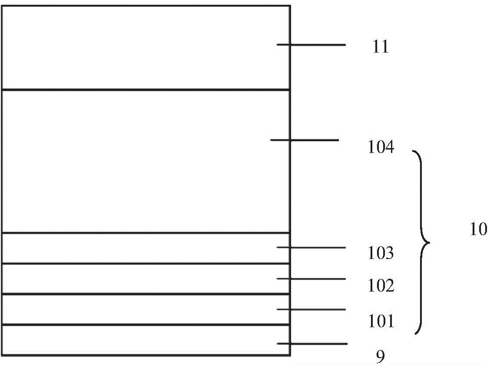
Image

Examples
Embodiment Construction
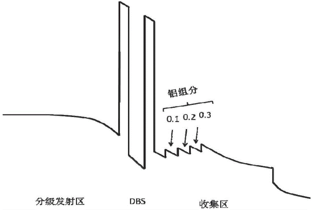
[0019] In order to realize a nano electronic device with extremely high frequency and working speed, the present invention proposes a resonant tunneling diode based on InGaAs / AlAs material, using n-type InP as the substrate; and heavily doped InGaAs to form the emission layer and the collection area; The strained InGaAs layer is used as the quantum well and AlAs is used as the barrier to form a double barrier single well structure (DBS); a mesa structure formed by n-type heavily doped high In composition InGaAs, and formed on the substrate and mesa respectively Au / Pi / Ti metal electrode.
[0020] The technical scheme of the present invention will be further explained below in conjunction with the drawings.
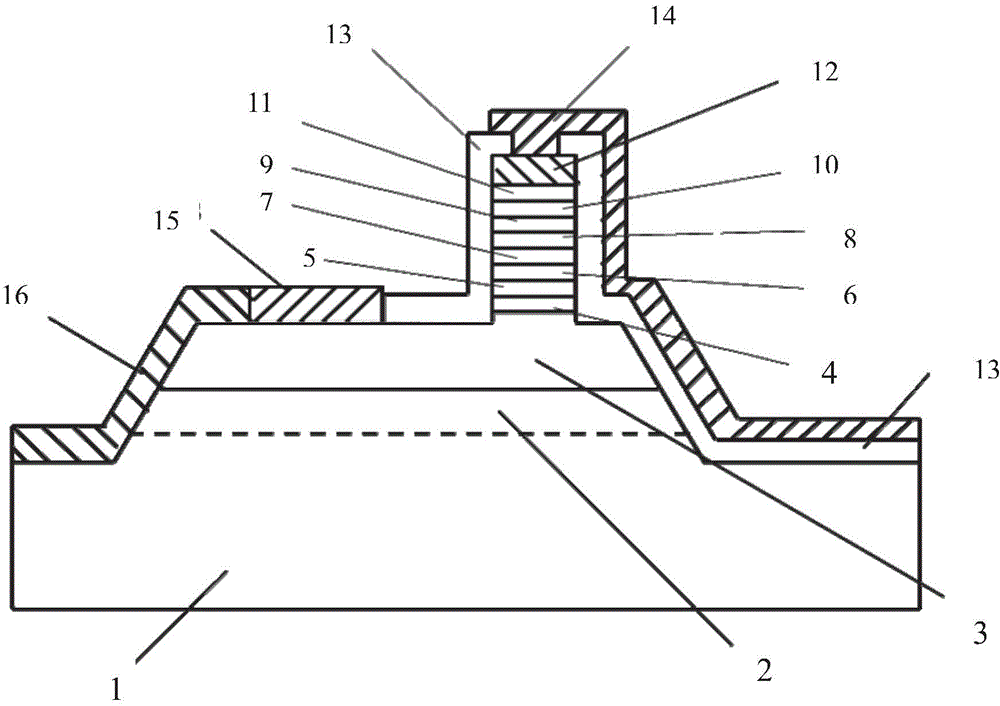
[0021] figure 1 Shown is a schematic diagram of the mesa structure of a resonant tunneling diode based on InGaAs / AlAs.
[0022] This InGaAs / AlAs-based resonant tunneling diode includes from bottom to top:
[0023] InP substrate layer 1;
[0024] An undoped InGaAs layer with a thick...
PUM
| Property | Measurement | Unit |
|---|---|---|
| Thickness | aaaaa | aaaaa |
Abstract
Description
Claims
Application Information