Antistatic device

a technology of antistatic devices and shielding components, applied in the direction of spark gap details, emergency protective arrangements for limiting excess voltage/current, relays, etc., can solve the problem of not being able to use an electrostatic protection component having a high capacitance, and achieve the effect of reducing discharge characteristics and reducing peak voltag

Inactive Publication Date: 2015-05-19
TDK CORPARATION
View PDF11 Cites 3 Cited by
  • Summary
  • Abstract
  • Description
  • Claims
  • Application Information

AI Technical Summary

Benefits of technology

[0022]With the present invention, an antistatic device is realized with which variations in the discharge characteristics can be reduced because corner portions of the discharge electrodes, where electric fields tend to concentrate, are covered with a discharge inducing portion and that has a lower peak voltage because a gap distance ΔG between opposing electrodes is controlled.

Problems solved by technology

Moreover, it has been not been possible to use an electrostatic protection component having a high capacitance in an antenna circuit or an RF module.

Method used


Image

  • Antistatic device
  • Antistatic device
  • Antistatic device

Examples


example 1

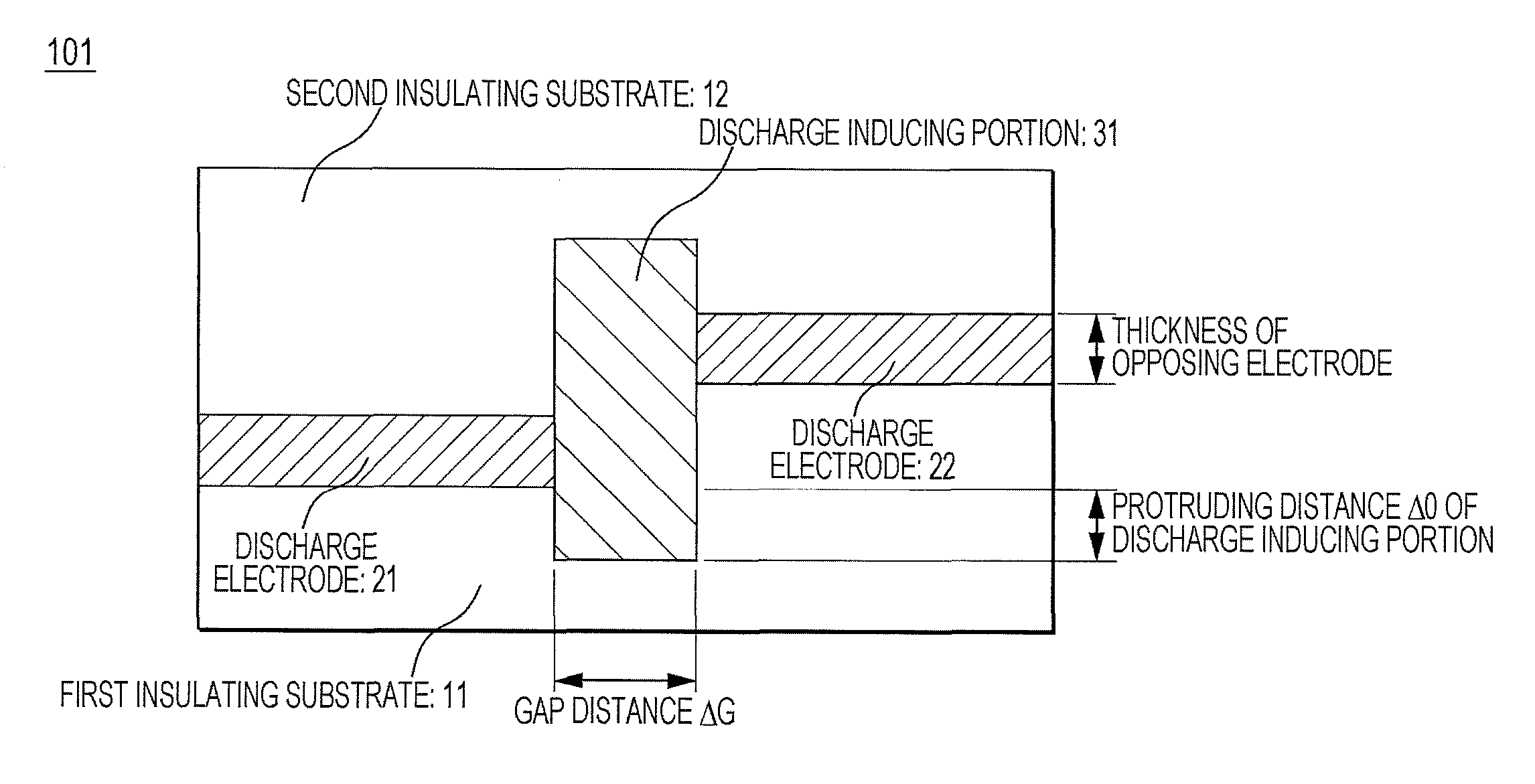
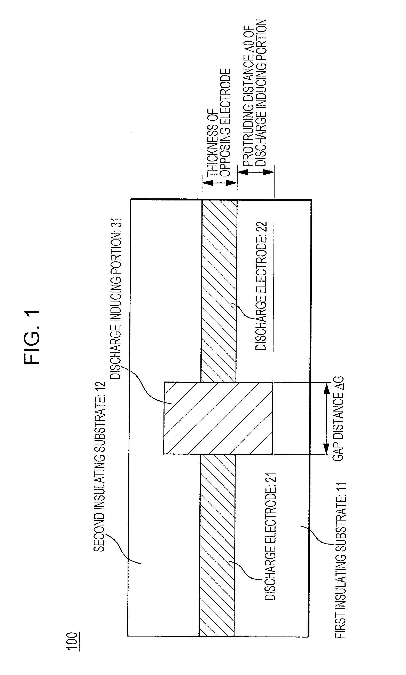
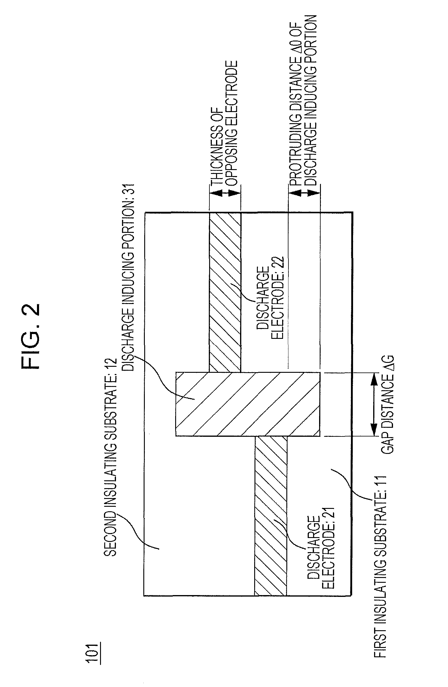
[0049]First, as illustrated in FIG. 3, a green sheet, which was made by forming a sheet from a material mainly composed of Al2O3 and a glass component, was prepared as the insulating substrate 11. A pattern of a strip-shaped electrode was formed by screen printing a Ag paste on the insulating surface Ila (FIG. 4) of the insulating substrate 11. The printed electrode had a length of 1 mm and a width of 0.4 mm. In order to adjust the thicknesses of the discharge electrodes after being fired, the thickness of a stencil was selected, and printing was performed so that the thickness of the discharge electrodes became 8 μm after being fired.

[0050]Next, as illustrated in FIG. 4, gap processing was performed so as to form a gap at the center of the strip-shaped electrode by using a femtosecond laser so that the gap distance became 5 μm and the depth of the gap became 2 μm after being fired. The depth of the gap after being fired was the same as the protruding distance ΔO (FIG. 1) of the dis...

example 2

[0056]An antistatic device 100 of Example 2 was obtained through a process the same as that of Example 1, except that gap processing was performed so that the gap distance became 15 μm after being fired.

example 3

[0057]The thickness of the stencil was changed so as to adjust the thickness of the opposing electrodes to 4 μm after being fired. Subsequently, an antistatic device 100 of Example 3 was obtained though a process the same as that of Example 1, except that gap processing was performed so that the gap distance became 15 μm after being fired and the protruding distance of the discharge inducing portion became 0.4 μm after being fired.


PUM


Abstract

To provide an antistatic device having a low capacitance, good discharge characteristics, and small variations in the discharge characteristics. In a so-called gap-type antistatic device in which a space between a pair of opposing electrodes is filled with an electrostatic protection material, a discharge inducing portion has protrusions protruding from interfaces between the opposing electrodes and the insulation substrates toward the insulation substrates and has a shape protruding on both sides of the insulation substrates. The relationship among the gap distance between the electrodes, the thicknesses of the opposing electrodes, and the protrusions of the discharge inducing portion is controlled under specific conditions.

Description

TECHNICAL FIELD[0001]The present invention relates to an antistatic device, and in particular, to an antistatic device that is suitable for use in a high-speed transmission system and for making a composite component integrated with a common mode filter.BACKGROUND ART[0002]In recent years, reduction in the size of and increase in the performance of electronic apparatuses have been progressing rapidly. Moreover, increase in transmission speed and reduction in drive voltage have been progressing rapidly as typically seen in high-speed transmission systems, such as USB 2.0, S-ATA 2, and HDMI. On the other hand, as reduction in the size of and reduction in the drive voltage of electronic apparatuses progress, the withstand voltages of electronic components used in the electronic apparatuses decrease. Therefore, it is technically important to protect electronic components from overvoltage, which is typified by an electrostatic pulse that occurs when a human body comes into contact with a...

Claims


Application Information

Patent Timeline
Patent Type & Authority Patents(United States)
IPC IPC(8): H01H47/00H01T1/20H01T4/12H02H9/06H05K9/00
CPCH01T4/12H01T1/20H05K9/0067H02H9/06
Inventor SUZUKI, SHINGONAKAMURA, JUNICHIASAKURA, KENSAKUFUJIMORI, TAKAHIRO
Owner TDK CORPARATION
Why Eureka
Try Eureka