Pad ESD Spreading Technique

a technology of esd and spreading, applied in the direction of emergency protective circuit arrangement, emergency protective arrangement for limiting excess voltage/current, electric discharge of very high current for a short duration, etc., can solve the problem of reducing the physical dimensions of circuit elements in many ics, for example in microprocessors, and reducing the maximum voltage. , the effect of improving esd performan

Active Publication Date: 2008-07-10
MICROCHIP TECH INC
View PDF27 Cites 5 Cited by
  • Summary
  • Abstract
  • Description
  • Claims
  • Application Information

AI Technical Summary

Benefits of technology

[0010]In one set of embodiments, a robust electrostatic discharge (ESD) structure for a variety of digital input / output (I / O) pads may be achieved. Output PMOS devices comprised in the output buffer of the pad and coupled between an I / O pad supply rail and the output pad may be enabled in response to an ESD event, to charge a pad capacitance (which, in some cases, may be approximately 3 pF) corresponding to the physical pad or pad cell, to spread out the energy generated by the ESD event, resulting in a lower peak voltage and therefore better ESD performance. By configuring all of the pads comprised within the system, (e.g. integrated circuit or part), to operate this way, the ESD energy may be shared by the respective pad capacitances corresponding to all the pads, thereby reducing the maximum voltage that may develop in the system as a result of the ESD event. This method may be employed as an additional technique to be used in conjunction with other established solutions, such as various clamp devices and clamp circuits, for example, allowing improved ESD performance over the established solutions used alone.
[0011]In one set of embodiments, an I / O pad circuit associated with a physical pad may comprise three main sections: an output buffer that may also include an ESD clamp device, a clamp control circuit, and a functional control block. The clamp control circuit may be supplied power by an ESD power rail that is activated by the energy of the ESD event, and may be triggered / enabled according to an RC time constant associated with a slope, or rise time, of a voltage pulse that may activate the ESD power rail. In an ESD event, the clamp control circuit may perform at least two different operations. It may turn on the clamp device in the output buffer, where the clamp device is coupled between the ESD power rail and a low supply rail, and may also send a signal to the functional control block, to instruct the functional control block to turn on the p-channel output device(s)—e.g. PMOS device(s)—comprised in the output buffer. By turning on the p-channel devices, while disabling n-channel devices—e.g. NMOS devices—that may also be comprised in the output buffer, and coupled to the PMOS device(s), the functional control block may operate to couple the high supply rail (i.e. the pad power rail) and its associated capacitance (such as all the other pad cells) to the pad affected by the ESD event, thus charge sharing the ESD pulse, thereby reducing the maximum voltage developed in the part comprising the pads. The reduced voltage correlates to improved part reliability. This technique may be used in conjunction with other established solutions, such as clamp devices and active clamp circuits, allowing improved ESD performance over other established solutions being used alone.

Problems solved by technology

ESD many times originates from build up of static charge near the IC or on a human handling the IC, leading to extremely high voltages developed near the IC, and typically results in an electrical discharge of very high current for a short duration.
Therefore, ESD poses a serious problem for semiconductor devices as it can potentially lead to malfunction and / or the destruction of an entire IC.
In addition, the physical dimensions of circuit elements in many ICs, for example in microprocessors, have seen a decrease with each new generation of manufacturing process.
Although smaller dimensions lead to an increase in IC operating speeds, they also have an adverse impact by increasing the sensitivity of circuit elements, such as field effect transistors (FETs), to high electric fields.
In the past, ESD protection circuits have had difficulty meeting these stringent requirements while maintaining adequate noise immunity and without increasing the required silicon area.

Method used


Image

  • Pad ESD Spreading Technique
  • Pad ESD Spreading Technique

Examples


Embodiment Construction

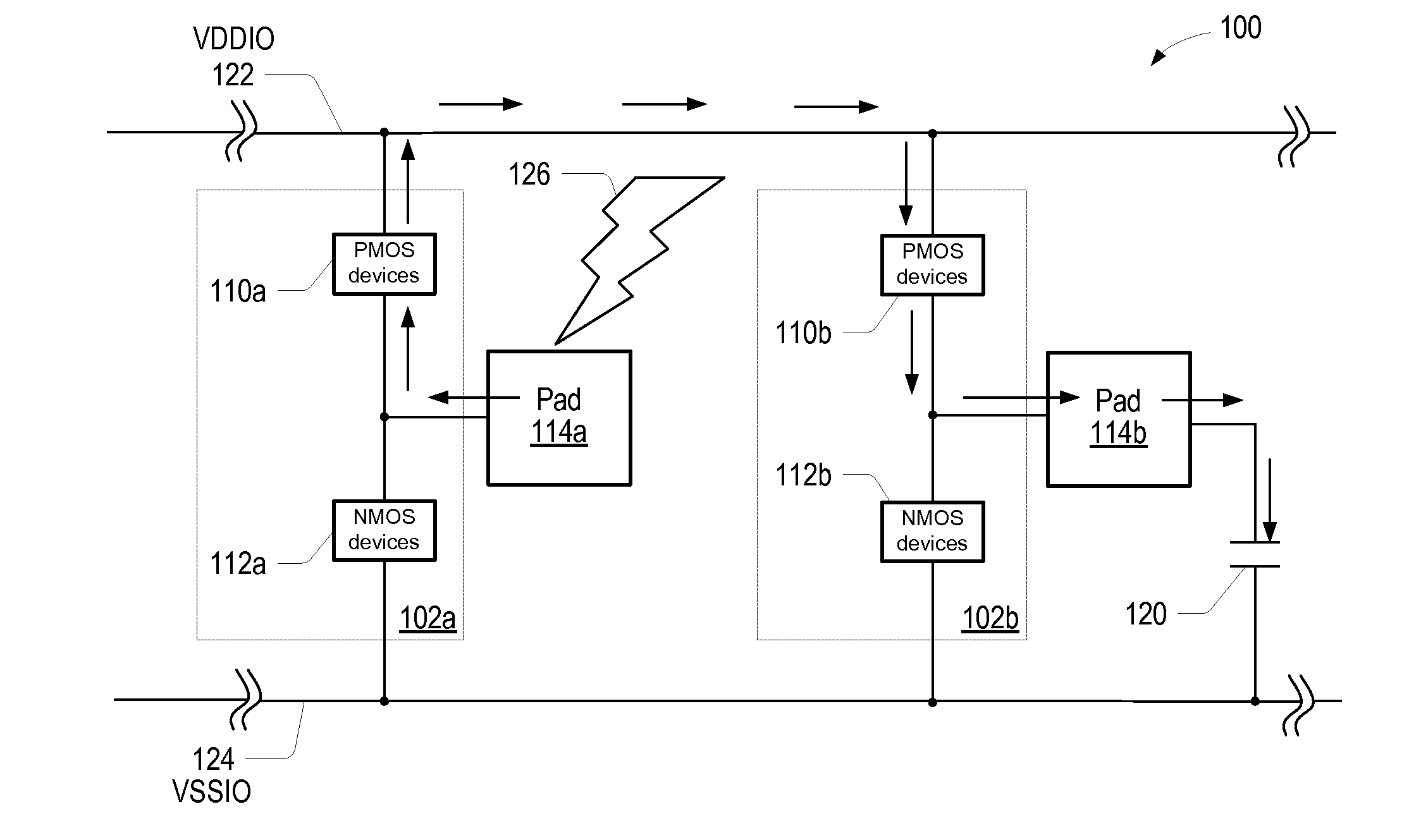
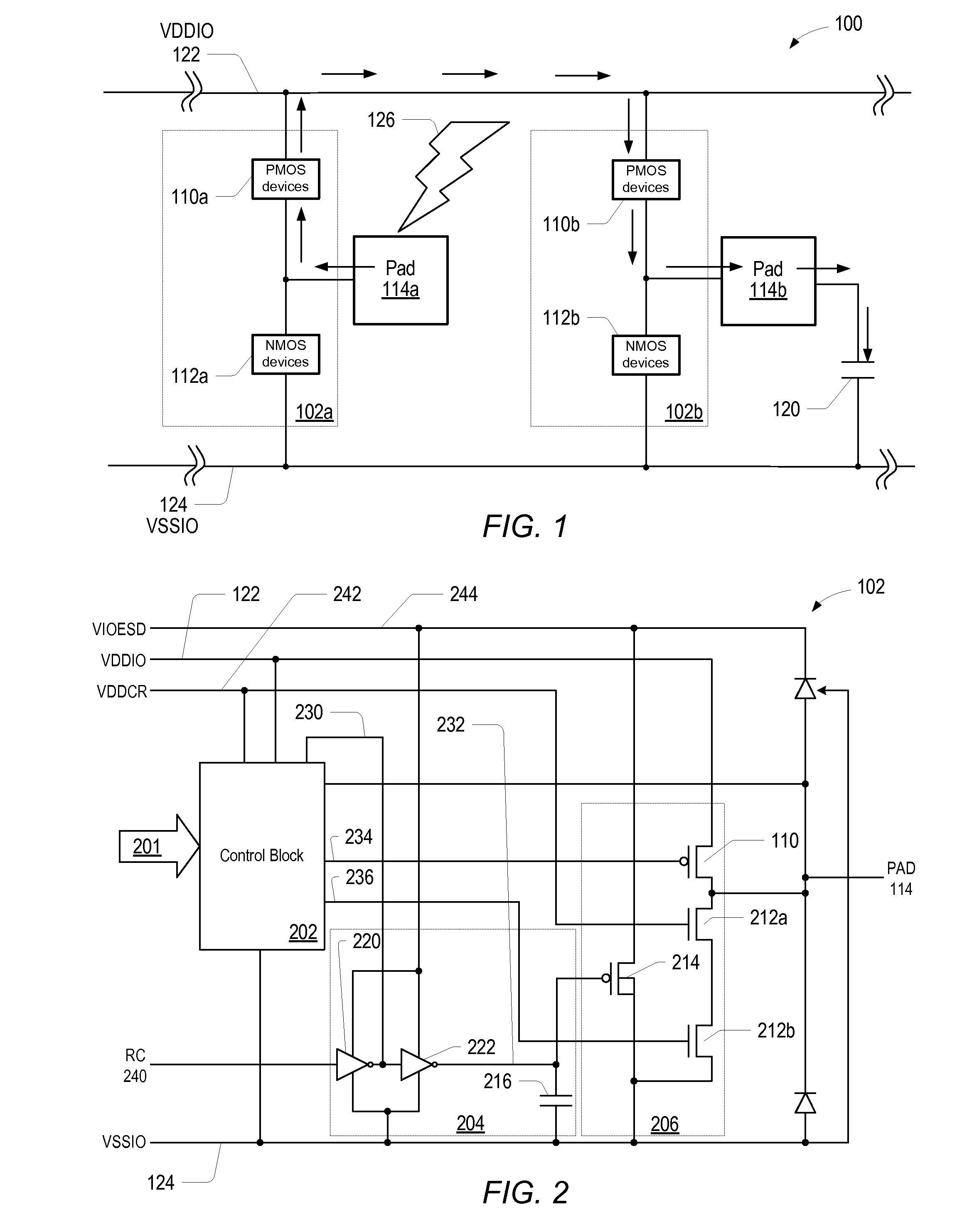
[0016]In one set of embodiments, a more robust electrostatic discharge (ESD) structure for a variety of variable input / output (I / O) pads may be realized. In one set of embodiments, output PMOS devices comprised in the output buffer of a pad, for example a digital I / O pad, may be enabled in response to an ESD event, to charge a pad capacitance (which may be approximately 3 pF) corresponding to the physical pad or pad cell, to spread out the ESD energy, which may result in a lower peak voltage and therefore better ESD performance. By configuring all of the pads comprised within the system, or integrated circuit, to operate this way, the ESD energy may be shared by the respective pad capacitances corresponding to all the pads, thereby reducing the maximum voltage that may develop in the system as a result of the ESD event (or of the energy of the ESD event). This method may be employed as an additional technique to be used in conjunction with other established solutions, such as variou...


PUM


Abstract

A system, e.g. an integrated circuit or part, may include a plurality of pads, e.g. digital I / O pads, each comprising a physical pad and associated pad circuit. In case of an ESD event affecting one or more of the digital I / O pads, PMOS devices configured in an output buffer section between an I / O pad supply rail and the physical output pad—within their respective pad circuits in the affected digital I / O pads—may all be turned on in response to the ESD event. This may allow the capacitance of each pad, in some cases approximately 3 pF capacitance per pad, to charge up, absorbing the energy of the ESD event and reducing the peak voltage the integrated circuit or part experiences as a result of the ESD event. The reduced peak voltage may be directly correlated with improved ESD performance of the product.

Description

BACKGROUND OF THE INVENTION[0001]1. Field of the Invention[0002]This invention relates generally to the field of integrated circuit design and, more particularly, to the design of protection circuitry for providing protection against damaging effects of Electrostatic Discharge (ESD).[0003]2. Description of the Related Art[0004]Integrated circuits (ICs) are typically manufactured with external connections—most commonly pins—for coupling to external devices, systems, signals and / or power supply voltages. More recently, IC design and manufacturing has been trending towards an increase in the density of internal components, most commonly transistors and device interconnects, with a concurrent decrease in the power supply voltage levels used in operating the ICs. As IC devices increase in density and operating supply voltage levels decrease, the IC devices may become more sensitive to the effects of electrostatic discharge (ESD).[0005]ESD many times originates from build up of static cha...

Claims


Application Information

Patent Timeline
Patent Type & Authority Applications(United States)
IPC IPC(8): H02H9/04
CPCH02H9/046
Inventor HOLLY, PATRICK J.RODRIGUEZ, DAVIDRICE, DAVID R.
Owner MICROCHIP TECH INC
Why Eureka
Try Eureka