
Display apparatus

a technology of display apparatus and display screen, which is applied in the field of display screen, can solve the problems of unavoidable luminance irregularities such as shading and crosstalk, and the decrease of the luminance of light emitted by the light emitting device, and achieve the effect of preventing luminance irregularities and obtaining high image quality

Inactive Publication Date: 2013-01-08
SONY CORP
View PDF15 Cites 12 Cited by
  • Summary
  • Abstract
  • Description
  • Claims
  • Application Information

AI Technical Summary

Benefits of technology

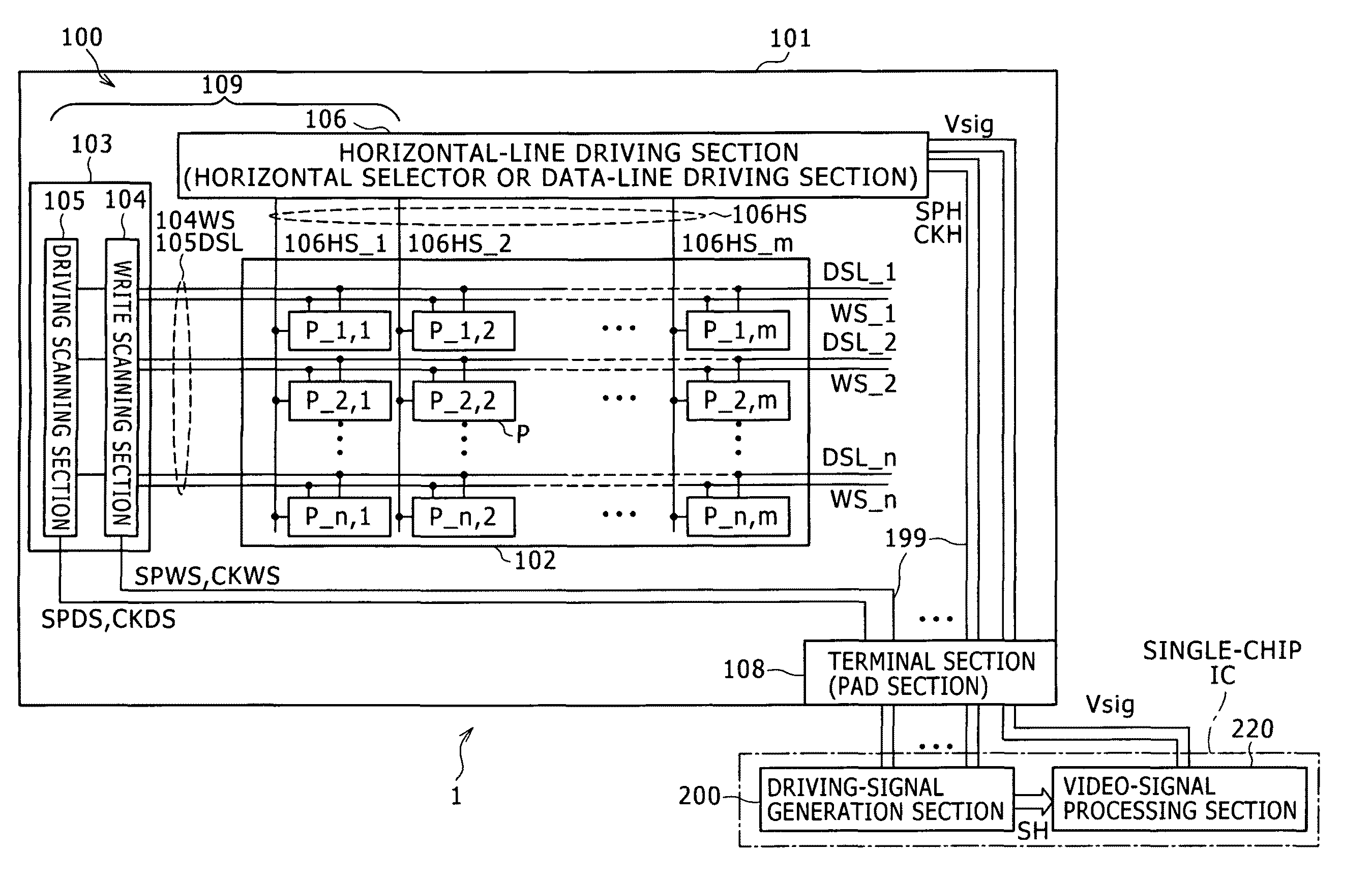
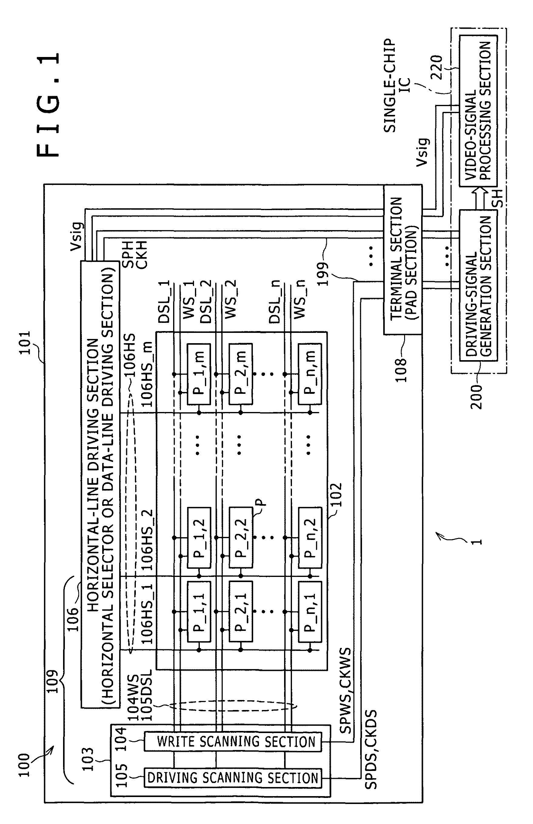
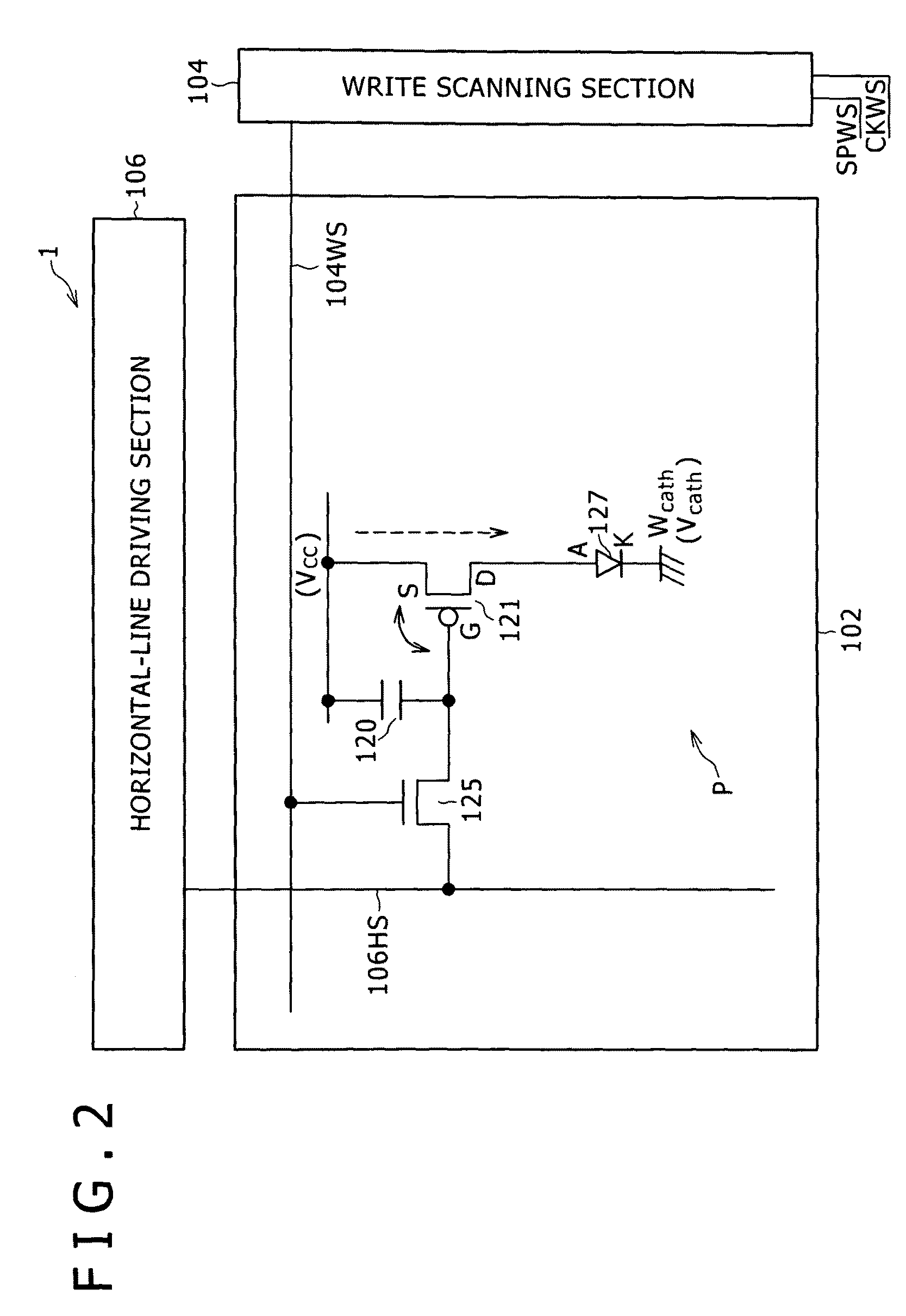
The present invention relates to a mechanism to prevent display irregularities caused by voltage drops on power-supply providing terminals of driving transistors. This is achieved by creating draw wires with adjusted resistance values to ensure uniform electric potentials on the power-supply providing terminals of the driving transistors. As a result, display apparatuses with high image quality can be obtained.

Problems solved by technology

Thus, the luminance of light emitted by the light emitting device also undesirably decreases gradually as well.
If the luminance of light emitted by the light emitting device decreases gradually, luminance irregularities such as shadings and crosstalk are generated unavoidably.

Method used


Image

  • Display apparatus
  • Display apparatus
  • Display apparatus

Examples


first embodiment

[0161]In a layout shown in the diagram of FIG. 12, on the other hand, the resistance of the draw wire 121DL on each pixel circuit P close to the driving scanning section 105 is made relatively large whereas the resistance of the draw wire 121DL on each pixel circuit P far away from the driving scanning section 105 is made relatively small. As shown in the diagram of FIG. 10, pixel circuits P close to the driving scanning section 105 are pixel circuits P1 and P4 whereas pixel circuits P far away from the driving scanning section 105 are pixel circuits P3 and P6.

[0162]That is to say, the length of the draw wire 121DL on any pixel circuit P is set at such a value that, the longer the distance between the driving scanning section 105 and the pixel circuit P, the smaller the resistance of the draw wire 121DL. To put it concretely, in the layout according to the first embodiment shown in the diagram of FIG. 12, the draw wire 121DL includes a first draw wire 121DL_1 connected to the drain...

second embodiment

[0165]FIG. 13A is an explanatory diagram serving as a model diagram referred to in description of a typical layout implementing the basic principle explained earlier by referring to the diagram of FIG. 10. In an implemented mechanism shown in the diagram of FIG. 10, the resistance of the draw wire 121DL on each pixel circuit P close to the driving scanning section 105 is made relatively large whereas the resistance of the draw wire 121DL on each pixel circuit P far away from the driving scanning section 105 is made relatively small. As shown in the diagram of FIG. 10, pixel circuits P close to the driving scanning section 105 are pixel circuits P1 and P4 whereas pixel circuits P far away from the driving scanning section 105 are pixel circuits P3 and P6.

[0166]That is to say, the width of the draw wire 121DL on any pixel circuit P is determined for every pixel circuit P so that, the longer the distance from the driving scanning section 105 to a pixel circuit P, the larger the value ...

third embodiment

[0169]FIG. 13B is an explanatory diagram serving as a model diagram referred to in description of a typical layout implementing the basic principle explained earlier by referring to the diagram of FIG. 10. In an implemented mechanism shown in the diagram of FIG. 10, the resistance of the draw wire 121DL on each pixel circuit P close to the driving scanning section 105 is made relatively large whereas the resistance of the draw wire 121DL on each pixel circuit P far away from the driving scanning section 105 is made relatively small. As shown in the diagram of FIG. 10, pixel circuits P close to the driving scanning section 105 are pixel circuits P1 and P4 whereas pixel circuits P far away from the driving scanning section 105 are pixel circuits P3 and P6.

[0170]That is to say, the length and width of the draw wire 121DL on any pixel circuit P are determined for every pixel circuit P so that, the longer the distance from the driving scanning section 105 to a pixel circuit P, the small...


PUM


Abstract

Disclosed herein is a display apparatus has a pixel array section including: pixel circuits which are each provided with a driving transistor and an electro-optical device and are laid out to form a matrix; and a draw wire provided in each of the pixel circuits to serve as a wire connecting the driving transistor to a power-supply providing line, wherein the resistance of the draw wire is relatively large in the pixel circuit close to a source applying a power-supply voltage to the power-supply providing line.

Description

BACKGROUND OF THE INVENTION[0001]1. Field of the Invention[0002]The present invention relates to a display apparatus employing pixel circuits each having an electro-optical device. The pixel circuit is also referred to merely as a pixel whereas the electro-optical device is also referred to as a display device or a light emitting device. To put it in more detail, the present invention relates to a display apparatus in which each of the pixel circuits employs an electro-optical device to serve as an electrically driven display device emitting light with a luminance varying in accordance with the magnitude of a driving signal driving the device and employs an active element for controlling the driving signal so that the display apparatus can be driven to display an image in pixel units.[0003]2. Description of the Related Art[0004]There is a display apparatus employing pixel circuits each having an electro-optical device serving as a display device which emits light with a luminance va...

Claims


Application Information

Patent Timeline
Patent Type & Authority Patents(United States)
IPC IPC(8): H04N5/66G09G3/20
CPCG09G3/3233G09G3/3208G09G2300/0819G09G2300/0842G09G2320/00G09G2320/043G09G2320/0233G09G3/3225G09G2320/0209H10K59/1315G09G3/2092
Inventor TANEDA, TAKAYUKIUCHINO, KATSUHIDELIDA, YUKIHITO
Owner SONY CORP
Learn More