Eight transistor soft error robust storage cell

a storage cell and transistor technology, applied in the field of eight transistor soft error robust storage cells, can solve the problems of 6t sram cells, vital building blocks of integrated circuits, yield, reliability and power consumption,

Active Publication Date: 2013-01-29
NYTELL SOFTWARE LLC
View PDF10 Cites 33 Cited by
  • Summary
  • Abstract
  • Description
  • Claims
  • Application Information

AI Technical Summary

Benefits of technology

[0010]A new storage cell configuration is introduced. The storage cell configuration allows for logical states to be stored with robustness against noise events such as soft errors. Various types of circuits can be implemented with this storage cell, including SRAM cells and flip-flops.

Problems solved by technology

Similarly, embedded SRAMs are a vital building block in integrated circuits.
SRAMs, in general, occupy a significantly large portion of the chip's die area, making it an important block in terms of area, yield, reliability and power consumption.
However the 6T SRAM cell, shown in FIG. 1, suffers from a relatively high vulnerability to soft errors.
This results in an erroneous state being stored, and the cell cannot recover.
If sufficient charge is collected the storage cell can switch its logical state, which is called a soft error.
For both circuits the data value stored in this structure can be susceptible to soft errors.
If a soft error transient is able to change the state of one node, the feedback of the dual-inverter storage cell will change the second node and result in erroneous data being stored.
The critical charge is the minimum amount of charge which will result in a soft error.
However, the addition of a large, area efficient coupling capacitor requires a special semiconductor manufacturing process.
Therefore this SRAM cell is not easily integrated into common Complementary Metal-Oxide-Semiconductor (CMOS) processes.
As a result, for Application Specific Integrated Circuits (ASICs) where embedded SRAM cells are widely realized using standard CMOS process, this approach is costly to implement.
Another problem with this approach is that while the capacitor increases the critical charge, it also makes the cell slower to write to.
This results in a lower frequency of operation, which is again not desirable.
Another drawback of this cell is that the extra capacitance which must be charged and discharged results in larger power consumption compared to the standard 6T SRAM cell.
However, the SRAM cell based on the DICE storage cell requires twice as many transistors to implement compared with the standard 6T SRAM circuit, making it expensive.
The result is that flip-flops which implement this storage cell require a greater number of transistors and use more power.

Method used


Image

  • Eight transistor soft error robust storage cell
  • Eight transistor soft error robust storage cell
  • Eight transistor soft error robust storage cell

Examples


Embodiment Construction

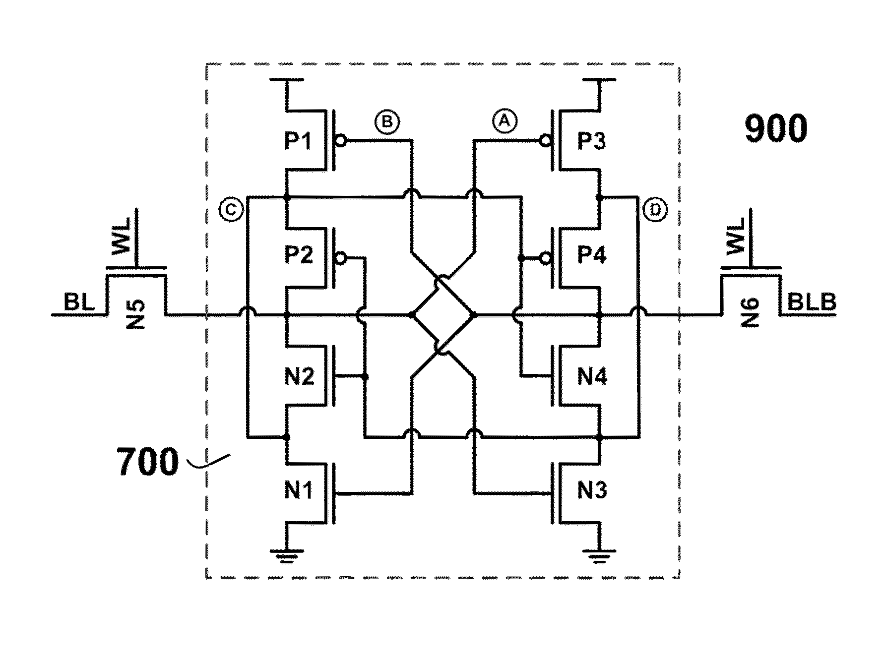
[0034]For convenience, like structures in drawings will be referenced by like numerals in the description. The following describes an eight transistor storage cell.

[0035]Referring to FIG. 7, an eight transistor storage cell in accordance with an embodiment of the present invention is illustrated generally by the numeral 700. The eight transistor storage cell 700 comprises four n-channel transistors N1, N2, N3 and N4 (known as drive transistors), four p-channel transistors P1, P2, P3 and P4 (known as load transistors) and four internal nodes A, B, C and D. Transistors N2, N4, P2 and P4 are given the name of core transistors. Transistors N1, N3, P1 and P3 are given the name of outer transistors. Nodes A and B are located at the drains of the core transistors and nodes C and D are located at the drains of the outer transistors.

[0036]In the storage cell 700 one logical value will be stored on nodes A and C and a complementary logical value will be stored on nodes B and D. Referring to F...


PUM


Abstract

A storage cell is provided with improved robustness to soft errors. The storage cell comprises complementary core storage nodes and complementary outer storage nodes. The outer storage nodes act to limit feedback between the core storage nodes and are capable of restoring the logical state of the core storage nodes in the event of a soft error. Similarly the core storage nodes act to limit feedback between the outer storage nodes with the same effect. This cell has advantages compared with other robust storage cells in that there are only two paths between the supply voltage and ground which limits the leakage power. An SRAM cell utilizing the proposed storage cell can be realized with two access transistors configured to selectively couple complementary storage nodes to a corresponding bitline. A flip-flop can be realized with a variety of transfer gates which selectively couple data into the proposed storage cell.

Description

[0001]The proposed Eight Transistor Storage Cell topology offers improved soft error robustness compared to the standard dual-inverter storage cell commonly used in 6T SRAM cells and static flip-flops. Compared with previously described soft error robust storage cells this topology allows smaller cells and reduced leakage power. This application claims the benefit of priority of U.S. Provisional Patent Application No. 61 / 193,503 filed Dec. 4, 2008 which is incorporated herein by reference in its entirety.BACKGROUND OF THE INVENTION[0002]SRAMs are one of the most popular ways to store data in electronic systems. Similarly, embedded SRAMs are a vital building block in integrated circuits. SRAMs are a preferred method of implementing embedded memories owing to higher speed, robust design, and ease of integration. SRAMs, in general, occupy a significantly large portion of the chip's die area, making it an important block in terms of area, yield, reliability and power consumption. With i...

Claims


Application Information

Patent Timeline
Patent Type & Authority Patents(United States)
IPC IPC(8): G11C11/00
CPCG11C11/412H03K19/007G11C11/4125
Inventor RENNIE, DAVIDSACHDEV, MANOJ
Owner NYTELL SOFTWARE LLC
Why Eureka
Try Eureka