Method for fabricating through substrate vias in semiconductor substrate

a technology of semiconductor substrate and via, which is applied in the direction of basic electric elements, electrical equipment, semiconductor devices, etc., can solve the problems of serious impact on the yield of the integrated circuit system

Active Publication Date: 2013-02-26
GLOBALFOUNDRIES INC
View PDF10 Cites 25 Cited by
  • Summary
  • Abstract
  • Description
  • Claims
  • Application Information

AI Technical Summary

Problems solved by technology

Thinning a large semiconductor wafer (typically 300 millimeters in diameter) to a thickness of 30-100 microns (μm) is a challenging process that can seriously impact the yield of the integrated circuit system.

Method used


Image

  • Method for fabricating through substrate vias in semiconductor substrate
  • Method for fabricating through substrate vias in semiconductor substrate
  • Method for fabricating through substrate vias in semiconductor substrate

Examples


Embodiment Construction

[0009]The following detailed description is merely exemplary in nature and is not intended to limit the invention or the application and uses of the invention. Furthermore, there is no intention to be bound by any expressed or implied theory presented in the preceding technical field, background, brief summary or the following detailed description.

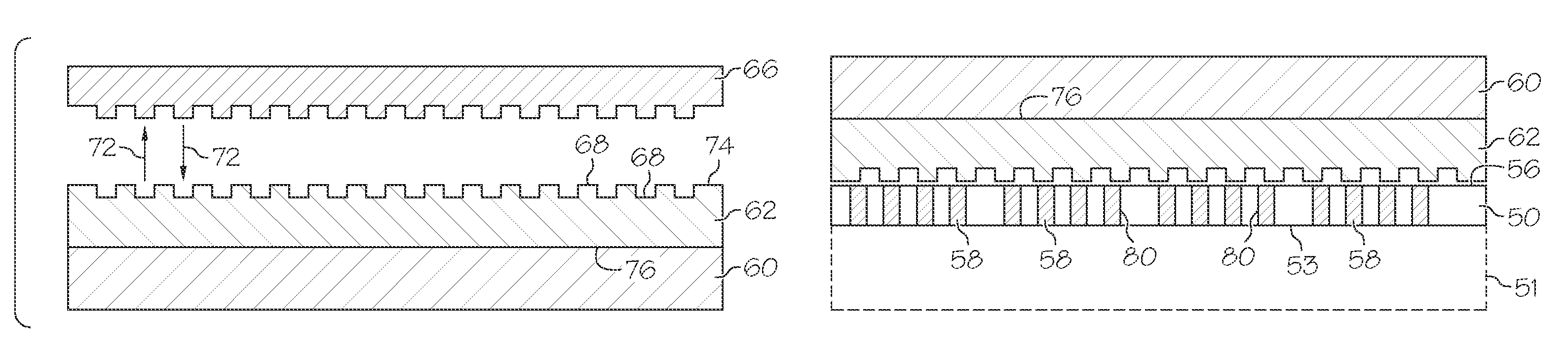
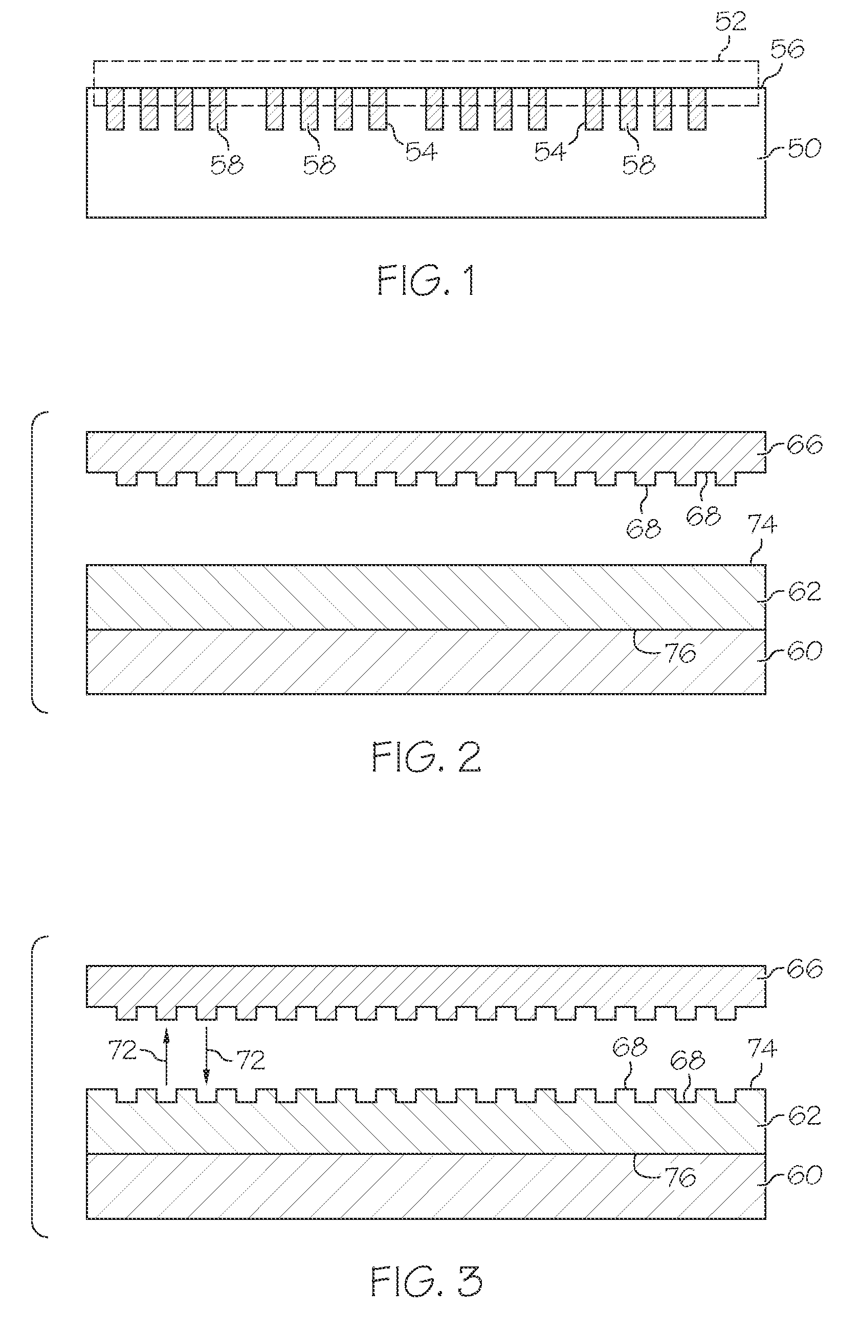
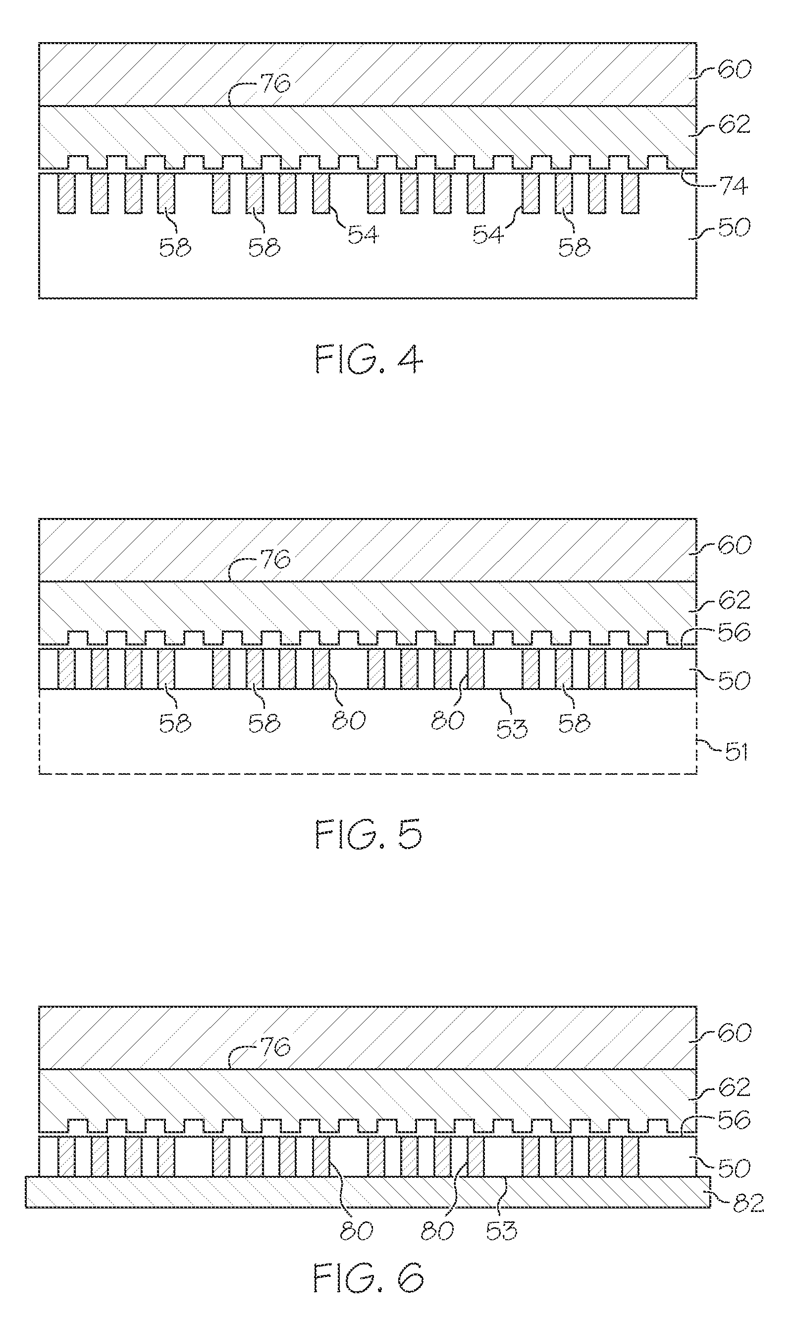
[0010]Fabricating integrated circuit (IC) systems often involves thinning of a semiconductor substrate in and on which a plurality of ICs have been formed. The thinning process may be part of the process of forming through substrate vias (TSVs) that facilitate interconnecting chips and substrates in stacked, three dimensional configurations. Thinning the semiconductor substrate requires bonding the substrate to a carrier wafer that provides physical support during the thinning as well as during processing of the back side of the substrate. Unfortunately the conventional bonding and subsequent de-bonding are major sources of yield loss in t...


PUM


Abstract

Methods are provided for fabricating integrated circuit systems that include forming integrated circuits in and on a semiconductor substrate. Via holes are etched into a front surface of the semiconductor substrate and are filled with a conductive material. A carrier wafer having a layer of adhesive thereon is provided and an imprinted pattern is formed in the layer of adhesive. The front surface of the semiconductor substrate is bonded to the carrier wafer with the patterned layer of adhesive. A portion of a back surface of the semiconductor substrate is removed to expose a portion of the conductive material and the thinned back surface is attached to a second substrate. The semiconductor substrate is then de-bonded from the carrier wafer.

Description

TECHNICAL FIELD[0001]The present invention generally relates to methods for fabricating integrated circuit systems, and more particularly relates to methods for fabricating integrated circuit systems including thinned substrates attached to other circuits or substrates.BACKGROUND[0002]Integrated circuit systems often include integrated circuits (ICs) that are attached to other ICs, interposer boards, or printed circuit boards in a stacked relationship. The IC system can include, for example, microprocessor circuits, memory circuits, analog circuits, and the like that are interconnected to take advantage of the unique attributes of the individual circuits. By vertically stacking the system components the size or footprint of the system can be minimized. Interconnection between the system components can be realized, in part, by through substrate vias (TSVs). Providing TSVs requires thinning the semiconductor substrate in and on which the IC is fabricated. Thinning a large semiconducto...

Claims


Application Information

Patent Timeline
Patent Type & Authority Patents(United States)
IPC IPC(8): H01L21/00
CPCH01L21/20H01L21/6835H01L21/76898H01L21/6836H01L2221/68318H01L2221/68327H01L2221/6834H01L2221/68381H01L2224/14
Inventor YIM, MYUNG JIN
Owner GLOBALFOUNDRIES INC
Why Eureka
Try Eureka