

Electron beam lithography apparatus and electron beam lithography method
a technology electron beam, which is applied in the field of electron beam lithography apparatus and electron beam lithography method, can solve the problems of difficult control, difficult to perform highly accurate exposure for a long time after, and reduce the throughput of exposure processing, and achieve high-accurate exposure processing continuously.
- Summary
- Abstract
- Description
- Claims
- Application Information
AI Technical Summary
Benefits of technology
Problems solved by technology
Method used
Image

Examples
Embodiment Construction
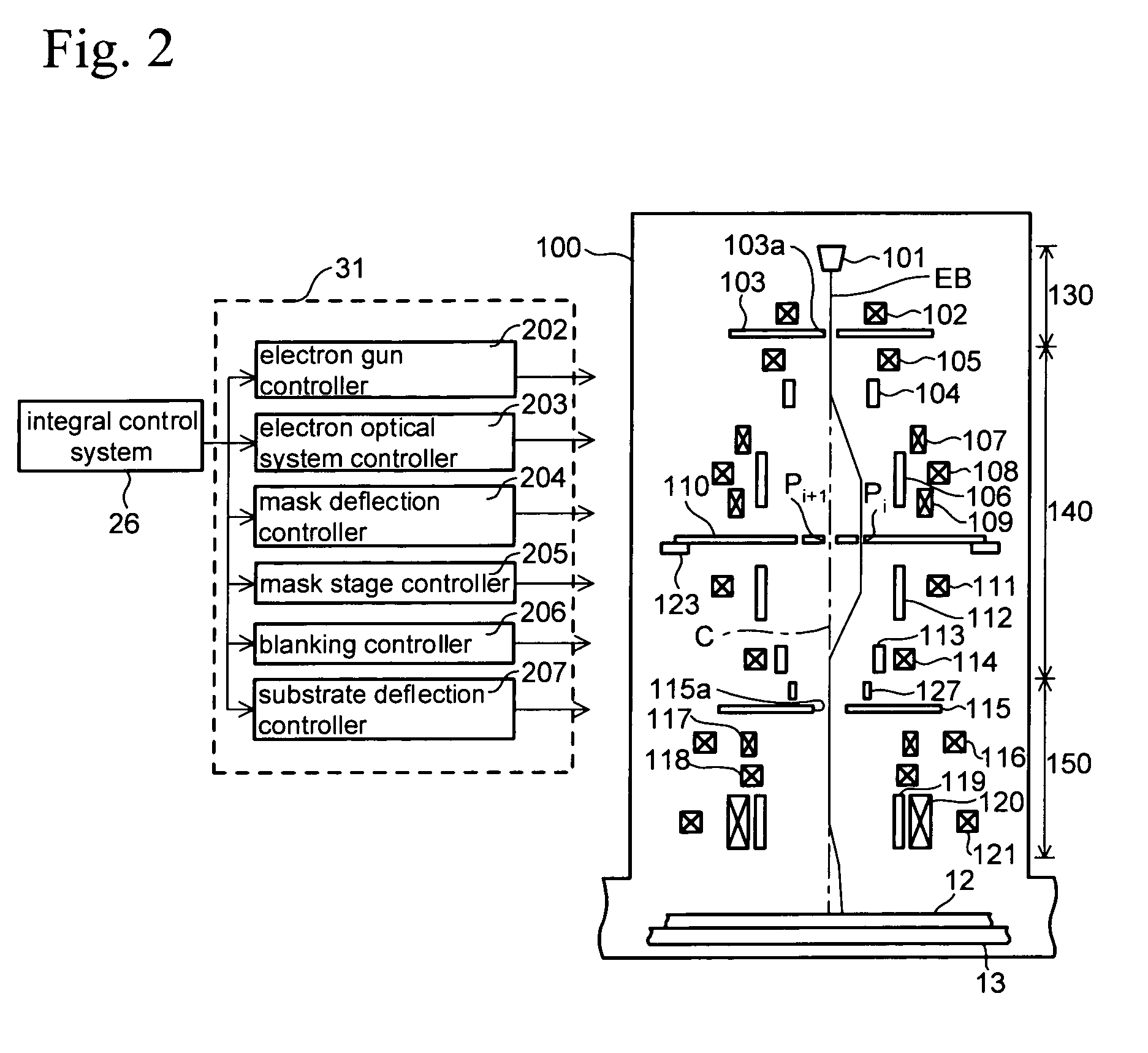
[0028]An embodiment of the present invention is described below with reference to the drawings. In the present embodiment, a multi-column electron beam exposure apparatus is described as an example of an electron beam lithography apparatus. First, with reference to FIGS. 1 to 3, the configuration of the multi-column electron beam exposure apparatus is described. Next, with reference to FIGS. 4 to 7, how to handle air pressure fluctuation is described. Next, with reference to FIG. 8, an electron beam exposure method is described as an example of an electron beam lithography method.
(Configuration of Main Body of Multi-Column Electron Beam Exposure Apparatus)
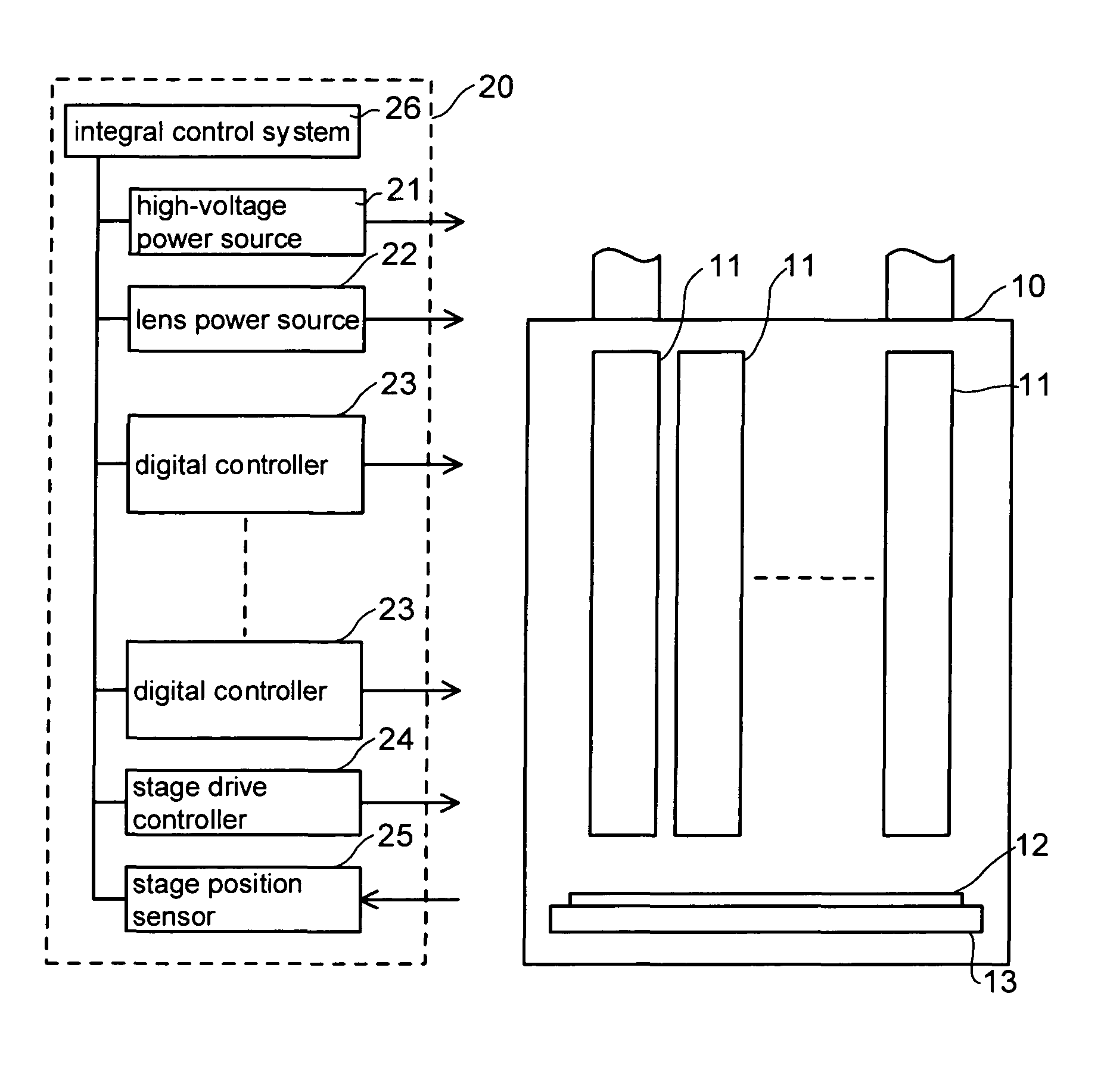
[0029]FIG. 1 is a schematic configuration diagram of the multi-column electron beam exposure apparatus according to the present embodiment.
[0030]The multi-column electron beam exposure apparatus roughly includes an electron beam column 10 and a controller 20 which controls the electron beam column 10. The electron beam column 10 is...
PUM
 Abstract
Description
Claims
Application Information