Coupled-loop chip antenna

a chip antenna and coupled loop technology, applied in the direction of antennas, electrically short antennas, antenna details, etc., can solve the problems of low integrity, large size, high cost during the fabrication process, etc., and achieve the effect of high integrity, small volume and preferable electrical characteristics

Inactive Publication Date: 2013-03-19
RRT TECH LTD
View PDF3 Cites 0 Cited by
  • Summary
  • Abstract
  • Description
  • Claims
  • Application Information

AI Technical Summary

Benefits of technology

[0007]In order to solve the problems in the prior art, the present invention is directed to a loop antenna, which is designed into a multi-band structure to create appropriate bandwidths, and is a chip antenna fabricated by a low-temperature co-fired ceramics (LTCC) process, thus having a relatively small volume of less than 100 mm3. Therefore, the coupled-loop chip antenna provided in the present invention has many preferable electrical characteristics including a high integrity, a low cost, and an appropriate bandwidth.

Problems solved by technology

The structure can be easily fabricated but the antenna has the disadvantages including an overly narrow bandwidth, a low integrity, and a large size.
However, the body of the loop antenna having a capacitive structure is a metal line segment with a plurality of three-dimensional bends, and is close to the ground, thus causing a high cost during the fabricating process.
Moreover, due to the special three-dimensional bend structure, the antenna in the wireless application product needs to be processed specially to integrate with other structures, and thus has no integrity.
I270236, entitled “Loop Antenna Having Capacitive Structure,” indeed solves the problems in the conventional unipole antenna and the loop antenna, but still fails to provide an antenna having various electrical characteristics including multiple frequency bands, appropriate bandwidth, a high integrity, a low cost, and a small size.
In addition, the chip antenna with a high integrity is a common implementation of antenna, but the characteristics of the antenna applying the chip process technique are always limited to an overly small chip size, for example, the size of the fabricated chip usually is in the range of millimeter (mm).
Therefore, the antenna structure in the range of millimeters may generate an unnecessary electric field and magnetic field coupling with the metal wire on other layers or other metal structures, which damages the original antenna performance and causes a narrow operating bandwidth.

Method used


Image

  • Coupled-loop chip antenna
  • Coupled-loop chip antenna
  • Coupled-loop chip antenna

Examples


Embodiment Construction

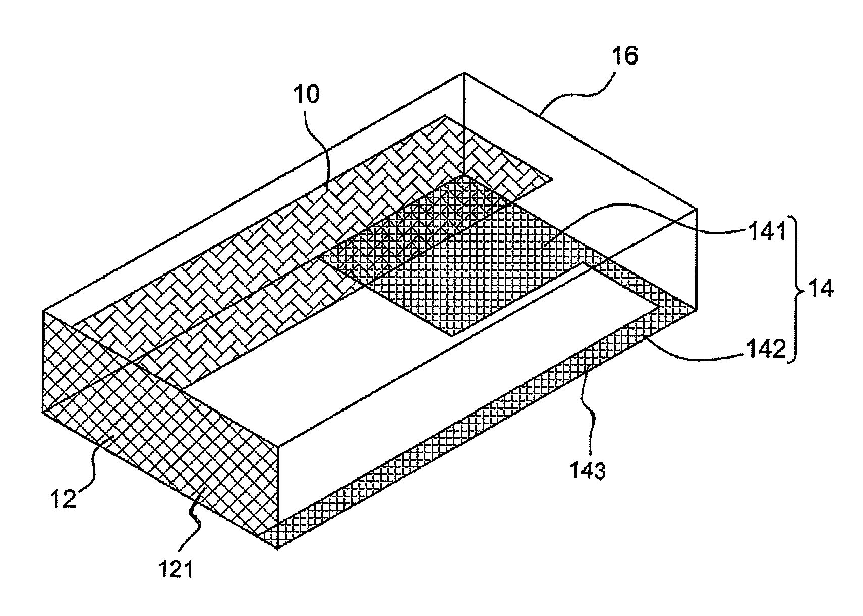
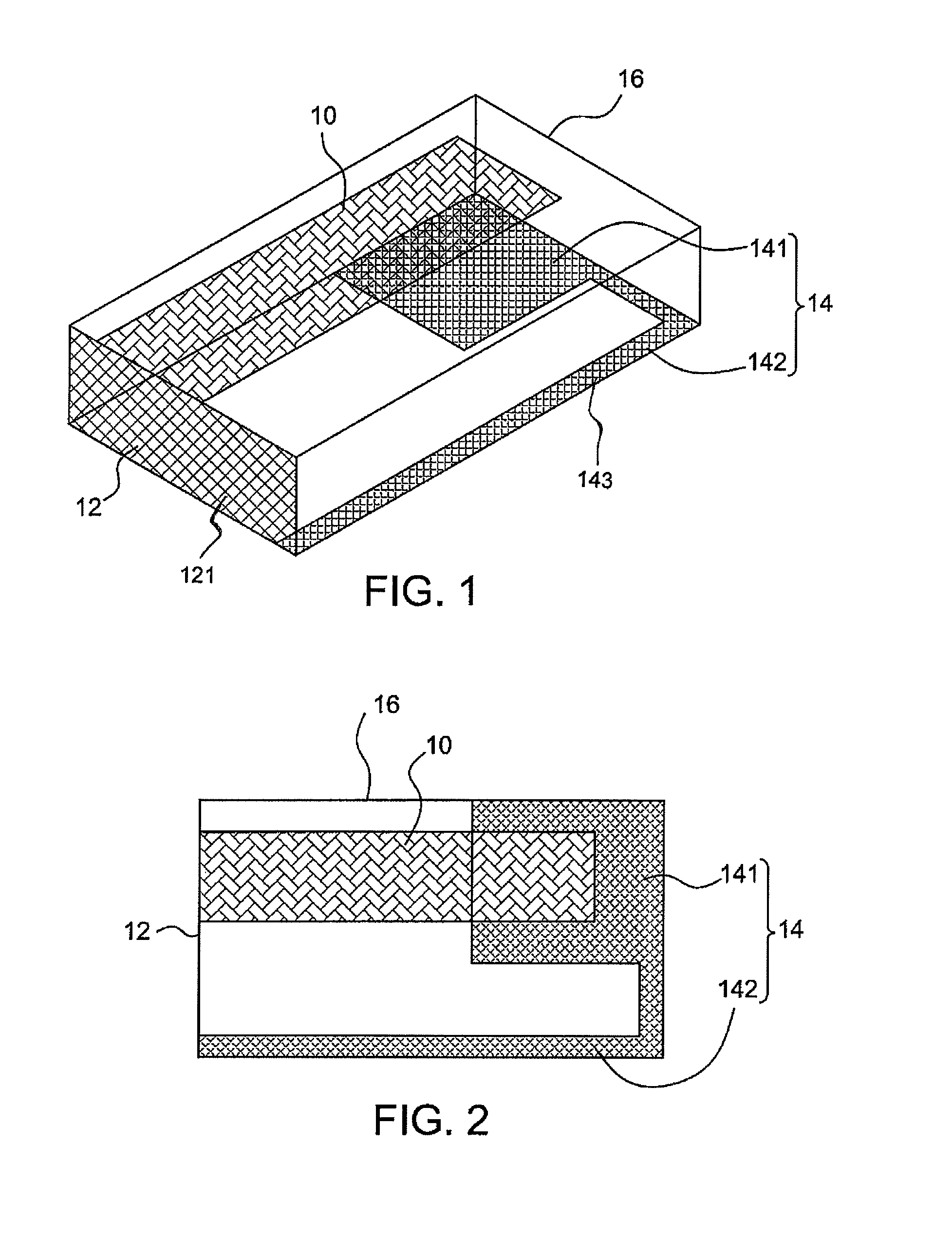
[0016]As shown in FIGS. 1 and 2, an coupled-loop chip antenna according to an embodiment of the present invention includes: a microwave substrate (16), being a hexahedron; a first conductive layer (10), disposed on an upper surface of the substrate (16) for forming a first loop; a second conductive layer (12), disposed on a first side surface of the substrate (16), and electrically connected to a feed-in point (121) and a ground point (143); and a third conductive layer (14), disposed on a lower surface of the substrate (16) For forming a second loop. The hexahedron is a cuboid, including a cube. The first conductive layer (10) and the second conductive layer (12) are electrically connected at the junction between the upper surface and the first side surface. The second conductive layer (12) and the third conductive layer (14) are electrically connected at the junction between the first side surface and the lower surface. The third conductive layer (14) includes a bent conductive la...


PUM


Abstract

A loop antenna for communication is provided, which includes a microwave substrate, being a hexahedron; a first conductive layer, disposed on an upper surface of the substrate for forming a first loop; a second conductive layer, disposed on a first side surface of the substrate, and electrically connected to a feed-in point and a ground point; and a third conductive layer, disposed on a lower surface of the substrate for forming a second loop. The first conductive layer and the second conductive layer are electrically connected at the junction between the upper surface and the first side surface, and the second conductive layer and the third conductive layer are electrically connected at the junction between the first side surface and the lower surface. The antenna also has an appropriate bandwidth for wireless communication application.

Description

BACKGROUND OF THE INVENTION[0001]1. Field of the Invention[0002]The present invention generally relates to a miniaturized microstrip antenna, in particular, to a coupled-loop chip antenna.[0003]2. Description of the Prior Art[0004]With rapid development of wireless communications recently, increasingly high requirements on the quality of the wireless communication continuously come up. Antenna is a dispensable communication element for all the wireless applications. In different wireless communication applications, although the requirements on the characteristics of the antenna are different, it can be summarized that, in order to obtain a stable communication quality, the antenna is required to be a communication element having various electrical characteristics such as multiple frequency bands, appropriate bandwidths (depending upon the type of the wireless communication application), a high integrity, a low cost, and a small size. Among the selections of various antenna structure...

Claims


Application Information

Patent Timeline
Patent Type & Authority Patents(United States)
IPC IPC(8): H01Q1/38
CPCH01Q7/00
Inventor TSAI, YUEH-LINTSAI, MENG HSUEHCHENG, CHIN HUANG
Owner RRT TECH LTD
Why Eureka
Try Eureka