Mask blank and method of manufacturing a transfer mask

a mask and mask technology, applied in the field of mask blanks and a manufacturing method of masks, can solve the problems of low conductivity of the target, defect tendencies, defect types, etc., and achieve the effects of excellent resist coating properties, reduced thickness, and high etching selectivity

Active Publication Date: 2013-04-02
HOYA CORP
View PDF5 Cites 2 Cited by
  • Summary
  • Abstract
  • Description
  • Claims
  • Application Information

AI Technical Summary

Benefits of technology

[0013]On the other hand, because of the reduction in thickness of the resist film, the resist film has no thickness margin for consumption during etching of the etching mask film and thus the accuracy of etching endpoint detection is getting very important in terms of CD (critical dimension) stability. However, there is a problem that the reflectance of the etching mask film made of the oxynitride of silicon is low for red laser light which is mainly used in the etching endpoint detection, thus making difficult the etching endpoint detection.
[0014]This invention has been made in view of such conventional circumstances and has objects firstly to provide a mask blank and a method of manufacturing a transfer mask, which can sufficiently achieve a reduction in thickness of a resist film, and secondly to provide a mask blank and a method of manufacturing a transfer mask, which can ensure high manufacturing stability.
[0060]According to this invention, by forming an etching mask film made of a material containing a transition metal, silicon, and at least one of nitrogen and oxygen on an upper surface of a light-shielding film formed on a transparent substrate and setting the content ratio of the transition metal to the total of the transition metal and the silicon in the etching mask film to less than 9%, it is possible to provide a mask blank and a method of manufacturing a transfer mask, in which the etching mask film has a high etching selectivity to a resist film so that it is possible to sufficiently achieve a reduction in thickness of the resist film by the use of such an etching mask film. Further, according to this invention, even if a surface treatment with a silane-based coupling agent is applied to a surface of the etching mask film, excellent resist coating properties are obtained with no occurrence of the above-mentioned conventional circular coating unevenness defects and thus it is possible to provide a mask blank and a method of manufacturing a transfer mask, which can ensure high manufacturing stability.

Problems solved by technology

In the case of the etching mask film of the oxynitride of silicon (e.g. SiON), the film formation is carried out by sputtering using a Si target, but there is a drawback that the conductivity of the target is low so that defects tend to occur.
Particularly in the case of the film formation by DC sputtering, defects tend to occur.
Further, in the case of, for example, the SiON film, the etching rate is somewhat low even in dry etching using a fluorine-based gas.
However, in the case of the etching mask film using the oxynitride of silicon as its material, there is a problem that since its etching selectivity to the resist film is low, the reduction in thickness of the resist film cannot be sufficiently achieved.
However, there is a problem that the reflectance of the etching mask film made of the oxynitride of silicon is low for red laser light which is mainly used in the etching endpoint detection, thus making difficult the etching endpoint detection.

Method used


Image

  • Mask blank and method of manufacturing a transfer mask
  • Mask blank and method of manufacturing a transfer mask
  • Mask blank and method of manufacturing a transfer mask

Examples


example 1

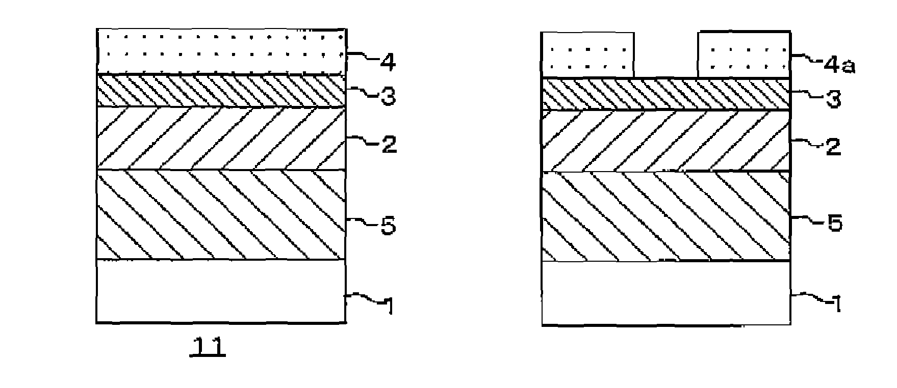
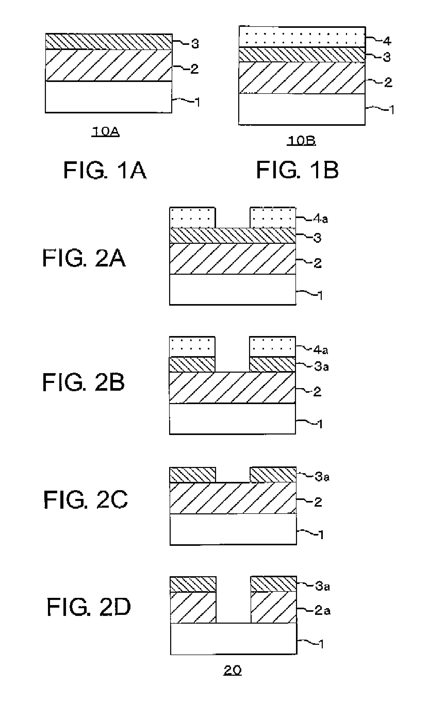
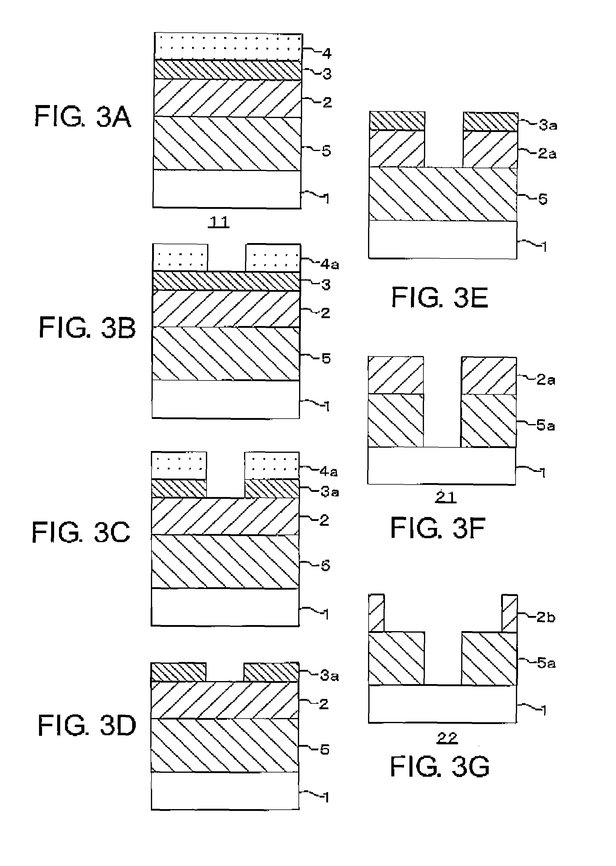
[0115]Using a single-wafer DC sputtering apparatus and using a chromium target as a sputtering target, reactive sputtering was carried out by setting the power of a DC power supply to 1.7 kW in a mixed gas atmosphere of argon, carbon dioxide, nitrogen, and helium (gas pressure 0.2 Pa; gas flow rate ratio Ar:CO2:N2:He=24:29:12:35), thereby forming a CrOCN layer with a thickness of 39 nm on a transparent substrate of a quartz glass. Then, using the chromium target, reactive sputtering was carried out by setting the power of the DC power supply to 1.7 kW in a mixed gas atmosphere of argon, nitrogen monoxide, and helium (gas pressure 0.2 Pa; gas flow rate ratio Ar:NO:He=27:18:55), thereby forming a CrON layer with a thickness of 17 nm. Finally, using the chromium target, reactive sputtering was carried out by setting the power of the DC power supply to 1.8 kW in a mixed gas atmosphere of argon, carbon dioxide, nitrogen, and helium (gas pressure 0.2 Pa; gas flow rate ratio Ar:CO2:N2:He=2...

example 2

[0123]Using a single-wafer DC sputtering apparatus and using a mixed target of molybdenum (Mo) and silicon (Si) (at % ratio Mo:Si=10:90) as a sputtering target, reactive sputtering (DC sputtering) was carried out by setting the power of a DC power supply to 2.8 kW in a mixed gas atmosphere of argon (Ar), nitrogen (N2), and helium (He) (gas pressure 0.3 Pa; gas flow rate ratio Ar:N2:He=5:49:46), thereby forming a MoSiN film with a thickness of 69 nm on a transparent substrate of a quartz glass. Then, the substrate formed with the MoSiN film was heat-treated (annealed) at 250° C. for 5 minutes, thereby forming a phase shift film for ArF excimer laser light (wavelength: 193 nm) in the form of a single layer composed mainly of molybdenum, silicon, and nitrogen. This phase shift film had a transmittance of 5.24% and a phase difference of 173.85 degrees for ArF excimer laser light (wavelength: 193 nm).

[0124]Then, using a chromium target as a sputtering target, reactive sputtering was carr...

example 3

[0134]Through the same processes as in Example 2, a phase shift film for ArF excimer laser light (wavelength: 193 nm) and a light-shielding film made of materials composed mainly of chromium were formed in this order on a transparent substrate of a quartz glass.

[0135]Then, using a mixed target of molybdenum (Mo) and silicon (Si) (at % ratio Mo:Si=4:96) as a sputtering target, a MoSiON film (etching mask film; Mo:1.8 at %, Si:37.2 at %, 0:12.9 at %, N:48.1 at %) was formed to a thickness of 10 nm in a mixed gas atmosphere of argon (Ar), oxygen, nitrogen, and helium.

[0136]Then, using a phase shift mask blank thus manufactured, a phase shift mask was manufactured. First, after applying an HMDS treatment to a surface of the mask blank under predetermined conditions, a chemically amplified positive resist film for electron beam writing (PRL009 manufactured by FUJIFILM Electronic Materials Co., Ltd.) was formed on the surface of the mask blank. The resist film was formed by spin coating u...


PUM

PropertyMeasurementUnit
thicknessaaaaaaaaaa
thicknessaaaaaaaaaa
wavelengthaaaaaaaaaa

Abstract

A mask blank includes a transparent substrate and a light-shielding film formed on the transparent substrate. The light-shielding film is made of a material composed mainly of a metal that is dry-etchable with a chlorine-based gas. A resist film is used to form a transfer pattern in the light-shielding film. An etching mask film is formed on an upper surface of the light-shielding film and is made of a material containing a transition metal, silicon, and at least one of nitrogen and oxygen. A content ratio of the transition metal to a total of the transition metal and the silicon in the etching mask film is less than 9%.

Description

[0001]This application is based upon and claims the benefit of priority from Japanese Patent Application No. 2010-007590, filed on Jan. 16, 2010, the disclosure of which is incorporated herein in its entirety by reference.TECHNICAL FIELD[0002]This invention relates to a mask blank and a method of manufacturing a transfer mask, which enable a reduction in thickness of a resist film.BACKGROUND ART[0003]Generally, fine pattern formation is carried out by photolithography in the manufacture of a semiconductor device. A number of substrates called transfer masks are normally used for such fine pattern formation. The transfer mask comprises generally a transparent glass substrate having thereon a fine pattern made of a metal thin film or the like. The photolithography is used also in the manufacture of the transfer mask.[0004]In the manufacture of a transfer mask by photolithography, use is made of a mask blank having a thin film (e.g. a light-shielding film) for forming a transfer patter...

Claims


Application Information

Patent Timeline
Patent Type & Authority Patents(United States)
IPC IPC(8): G03F1/50G03F1/32G03F1/68G03F1/80
CPCG03F1/54G03F1/80G03F1/50H01L21/0274
Inventor HASHIMOTO, MASAHIROIWASHITA, HIROYUKIHIROMATSU, TAKAHIRO
Owner HOYA CORP
Why Eureka
Try Eureka