Semiconductor device and process for production thereof

a technology of semiconductor devices and semiconductors, applied in the direction of semiconductor devices, basic electric elements, electrical equipment, etc., can solve problems such as avalanche breakdown, and achieve the effects of reducing channel resistance, reducing channel length, and increasing reliability

Inactive Publication Date: 2013-04-16
PANASONIC CORP
View PDF20 Cites 46 Cited by
  • Summary
  • Abstract
  • Description
  • Claims
  • Application Information

AI Technical Summary

Benefits of technology

[0031]According to the present invention, since a second doped region of the first conductivity type is provided, carriers supplied from the second doped region of the first conductivity type can prevent a depletion layer, which is formed in a drift layer through a contact with a body region, from expanding. Thus, the increase in channel length can be minimized and electrons can flow into the drift layer through the second doped region of the first conductivity type. As a result, the channel resistance can be reduced effectively.
[0032]In addition, since a third doped region of the first conductivity type is further provided, the overconcentration of an electric field toward the gate insulating film at a middle point between the body regions, which would otherwise be caused by the voltage applied to the second ohmic electrode when the semiconductor device is OFF state, can be lessened. Consequently, the breakdown voltage and the reliability can be both increased.

Problems solved by technology

As a result, an avalanche breakdown will happen.

Method used


Image

  • Semiconductor device and process for production thereof
  • Semiconductor device and process for production thereof
  • Semiconductor device and process for production thereof

Examples


experimental examples

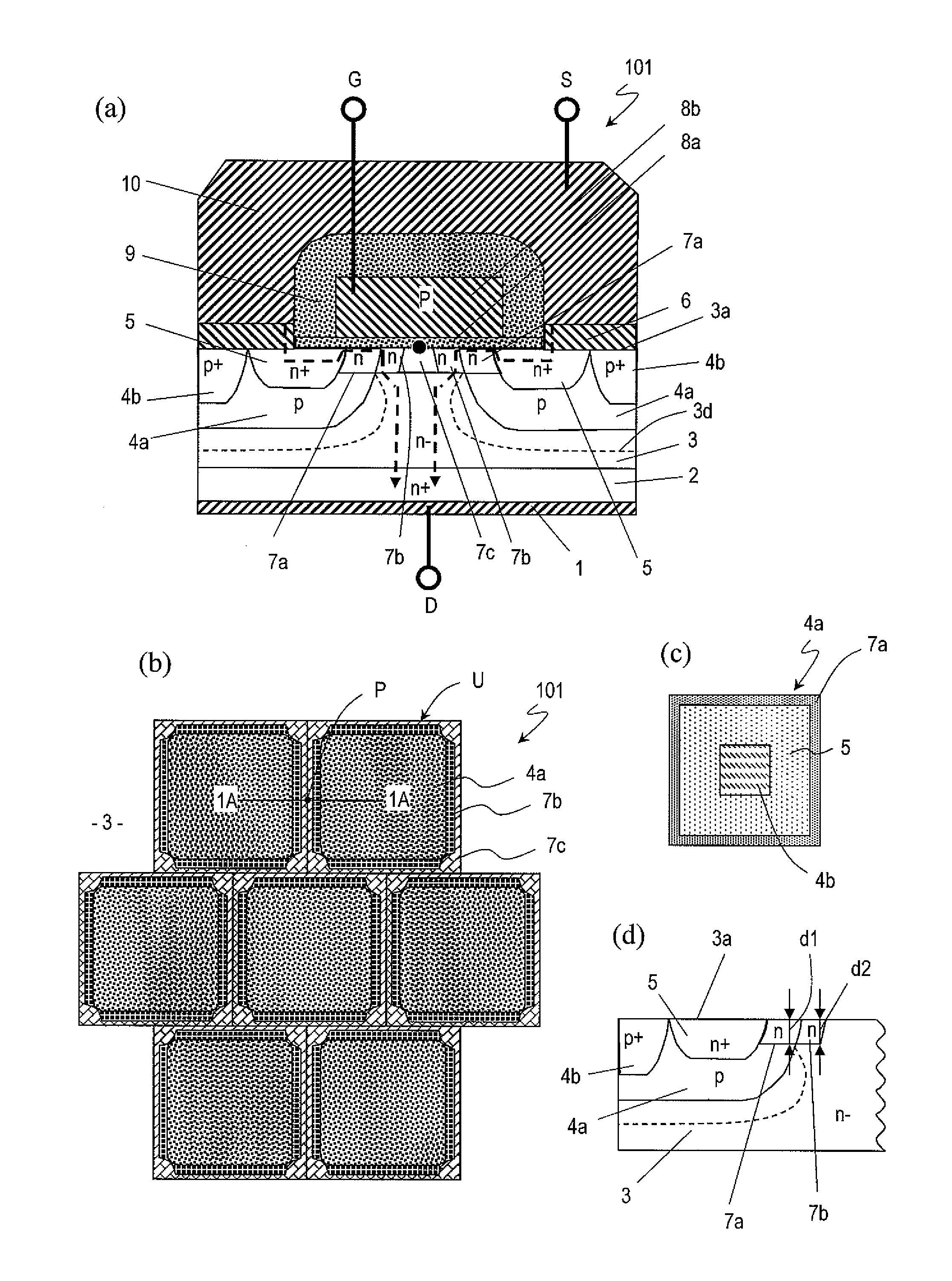
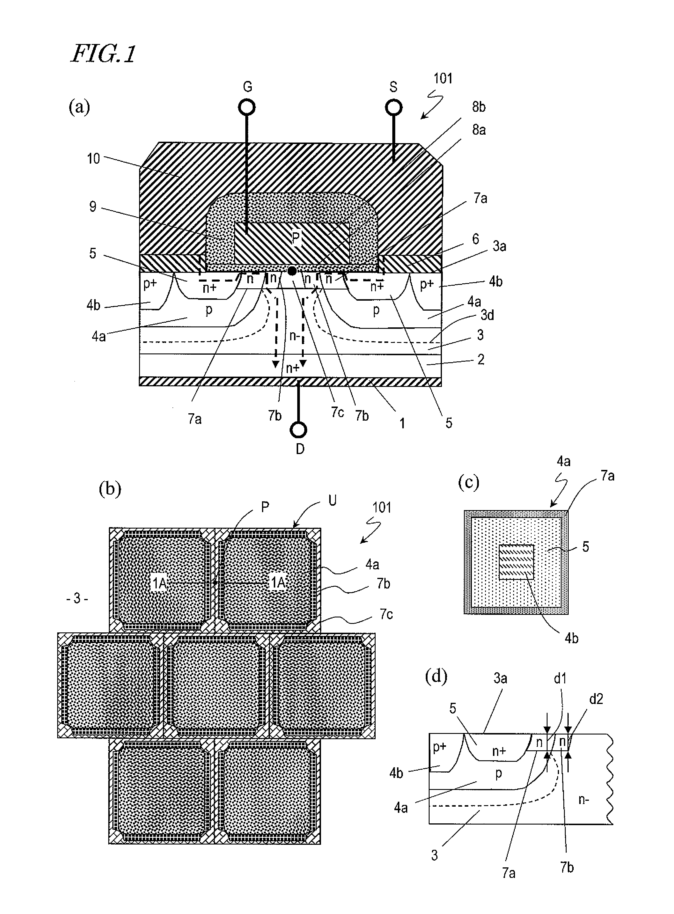
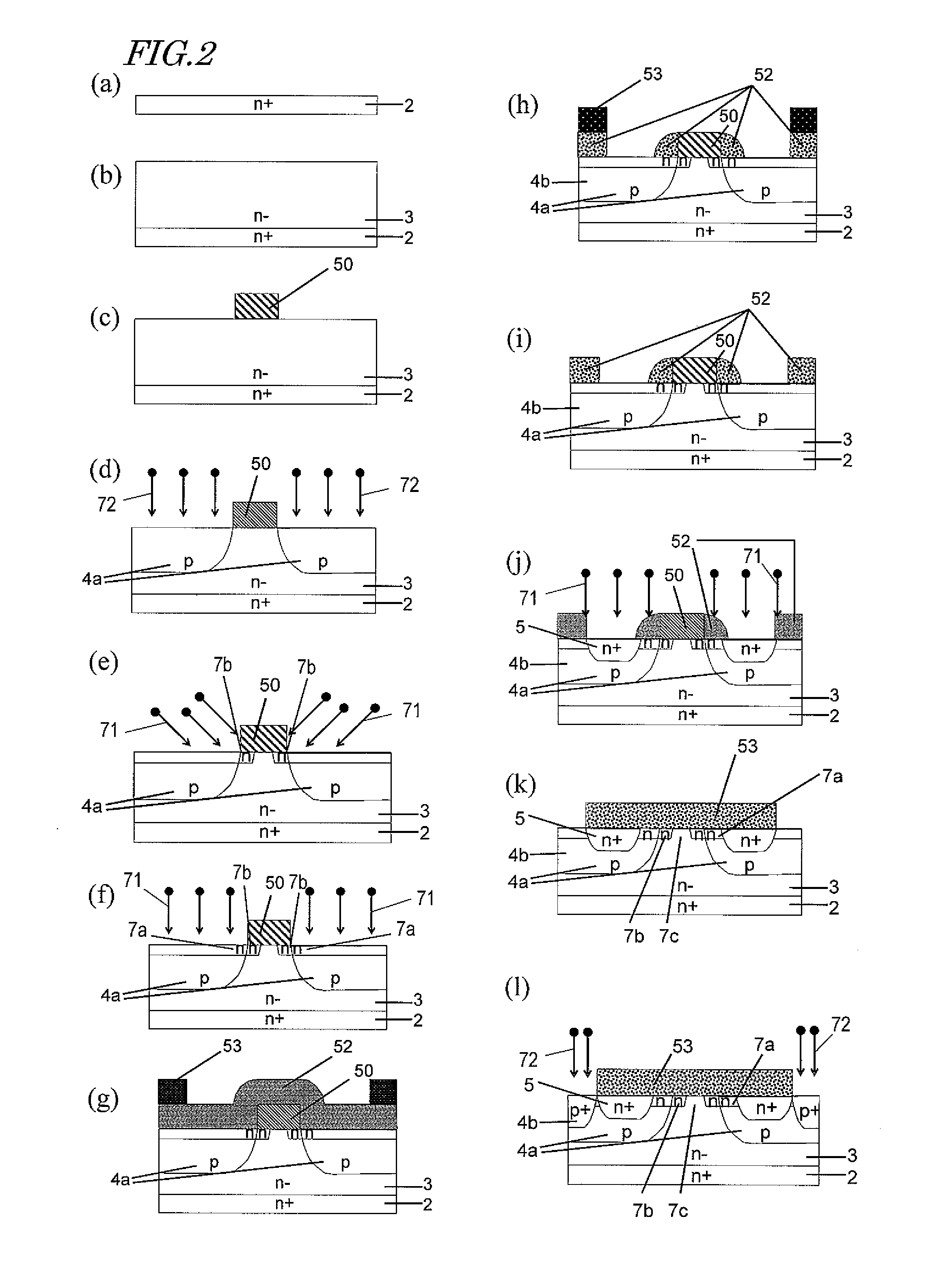
[0094]The present inventors carried out experiments to examine how a variation in the dopant concentrations of the second doped region 7b of the first conductivity type and the body region 4a would affect the channel resistance of the MISFET 101 of the first preferred embodiment. The results are as follows.

[0095]Suppose the size of each unit cell is indicated by Xcell and the interval between the respective first n-type doped regions 5 of two adjacent unit cells and the interval between the respective second n-type doped regions 7a thereof as measured in the direction in which the unit cells are arranged are indicated by a+2Lg and a, respectively, as shown in FIG. 7. The width of the second n-type doped region 7a as measured in the direction in which the unit cells are arranged is indicated by Lg representing the channel length. The numerical values that were used to make a calculation are shown in the following Table 1:

[0096]

TABLE 1ItemSignUnitValueUnit cell sizeXcellμm9.6Interval ...


PUM


Abstract

The semiconductor device of this invention has unit cells, each of which includes: a substrate; a drift layer on the substrate; a body region in the drift layer; a first doped region of a first conductivity type in the body region; a second doped region of the first conductivity type arranged adjacent to the body region and in a surface region of the drift layer; a third doped region of the first conductivity type arranged between two adjacent unit cells' second doped region of the first conductivity type and in the surface region of the drift layer to contact with the second doped region of the first conductivity type; a gate insulating film arranged to contact with the surface of the drift layer at least between the first and second doped regions of the first conductivity type; a gate electrode on the gate insulating film; and first and second ohmic electrodes. The dopant concentration of the third doped region of the first conductivity type is lower than that of the second doped region of the first conductivity type and equal to or higher than that of the drift layer.

Description

TECHNICAL FIELD[0001]The present invention relates to a semiconductor device and more particularly relates to a silicon carbide semiconductor device and a method for fabricating the device.BACKGROUND ART[0002]A wide-bandgap semiconductor has attracted a lot of attention as a semiconductor material that could be potentially used to make a semiconductor device that has a high breakdown voltage and that can make a huge amount of current flow through it (i.e., a so-called “power device”). Among other things, silicon carbide (SiC) has a much higher dielectric breakdown voltage than any other wide-bandgap semiconductor, and therefore, is expected to be the best semiconductor material to make a next-generation low-loss power device. As a quality silicon dioxide (SiO2) film can be formed on SiC by thermal oxidation, an insulated gate SiC power MISFET (metal-insulator-semiconductor field effect transistor) that uses such a silicon dioxide film as its gate insulating film is currently under d...

Claims


Application Information

Patent Timeline
Patent Type & Authority Patents(United States)
IPC IPC(8): H01L29/66H01L21/04
CPCH01L21/047H01L29/0847H01L29/66068H01L29/7828H01L21/0465H01L29/0696H01L29/1608
Inventor YAMASHITA, KENYA
Owner PANASONIC CORP
Why Eureka
Try Eureka