Liquid crystal display device

a display device and liquid crystal technology, applied in non-linear optics, instruments, optics, etc., can solve the problems of insufficient alignment control force, low contrast ratio, narrow viewing angle, etc., and achieve no roughness, suppressed variation in brightness, and high quality display

Active Publication Date: 2013-04-16
SHARP KK
View PDF19 Cites 2 Cited by
  • Summary
  • Abstract
  • Description
  • Claims
  • Application Information

AI Technical Summary

Benefits of technology

[0031]A liquid crystal display device of the present invention includes fishbone-type electrodes which have branch portions of the above-specified width or fishbone-type electrodes in which the space between adjacent branch portions has the above-specified value. Therefore, the abnormal alignment and alignment shift of the liquid crystal are suppressed so that the alignment direction of the liquid crystal in each pixel can be stabilized to be in a correct direction. Thus, high quality display with no roughness is possible in which the variation in transmittance across the display surface is smaller than about 10%.
[0032]In a liquid crystal display device of the present invention, one pixel includes two regions between which the widths of branch portions of the fishbone-type electrode or the spaces between adjacent branch portions are different. Therefore, the variation in brightness is suppressed, and high quality display with excellent gray scale and viewing angle characteristics is achieved.

Problems solved by technology

If the slit width is narrower than this, sufficient alignment control force cannot be obtained.
The CPA mode which utilizes the ¼-wave plates achieves high transmittance but disadvantageously provides a low contrast ratio and a narrow viewing angle as compared with the MVA mode.
Abnormal alignment of the liquid crystal, or such a phenomenon that the liquid crystal alignment direction becomes unstable, can occur depending on the shape or size of the linear electrode portions or the shape or size of the plurality of slits extending parallel to the linear electrode portions (also referred to as “linear space portions”), resulting in the problems of variation in transmittance across the display surface, display unevenness, and abnormal gray scale.
However, the shape and size of the linear electrode portions and slits which are optimum for achieving such high transmittance characteristics has not been researched.
Also, the fishbone-type electrodes have not been researched as to what setting of the relationship between the width of the linear electrode portions and the width of the slits can achieve the best transmittance characteristics.

Method used


Image

  • Liquid crystal display device
  • Liquid crystal display device
  • Liquid crystal display device

Examples


embodiment 1

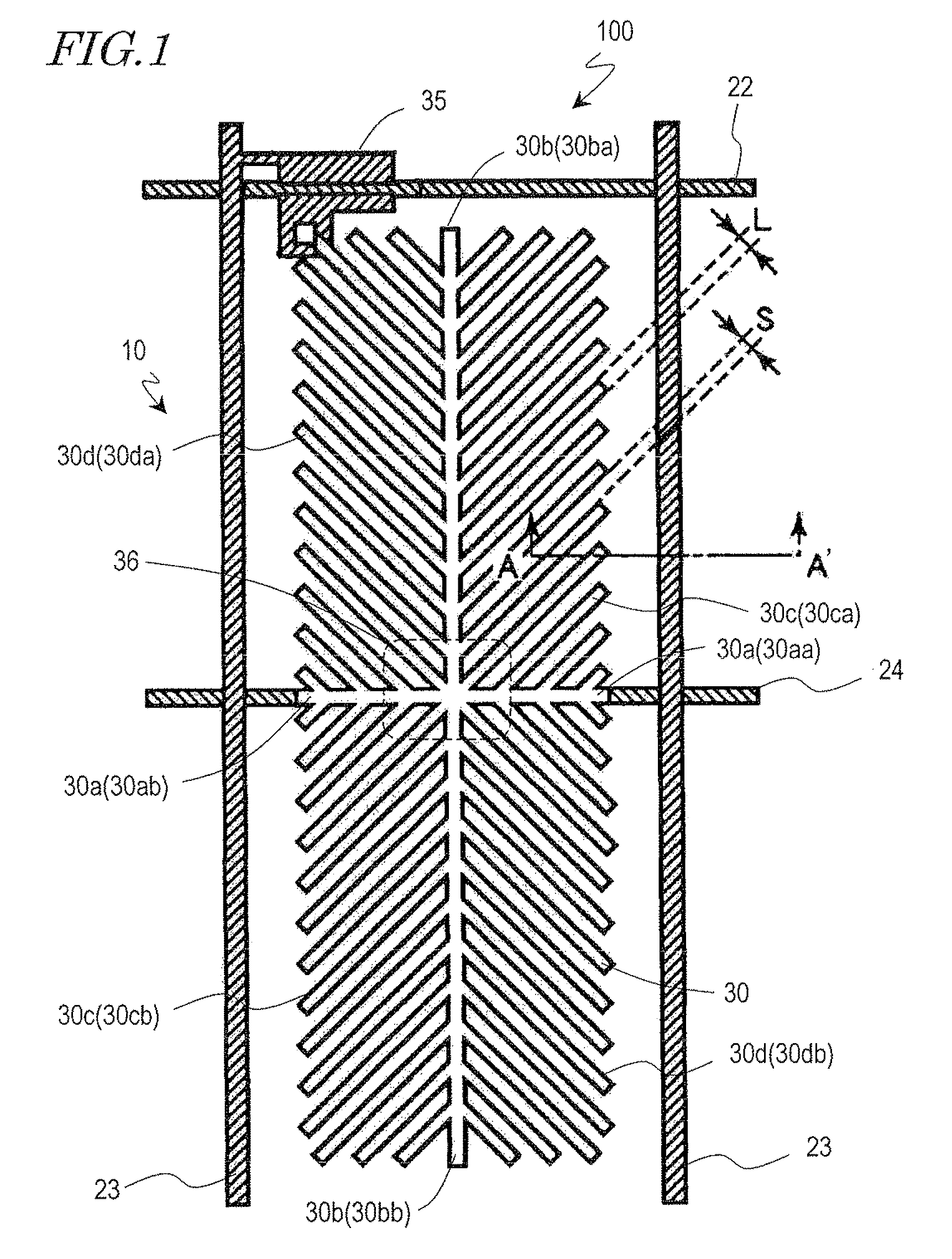
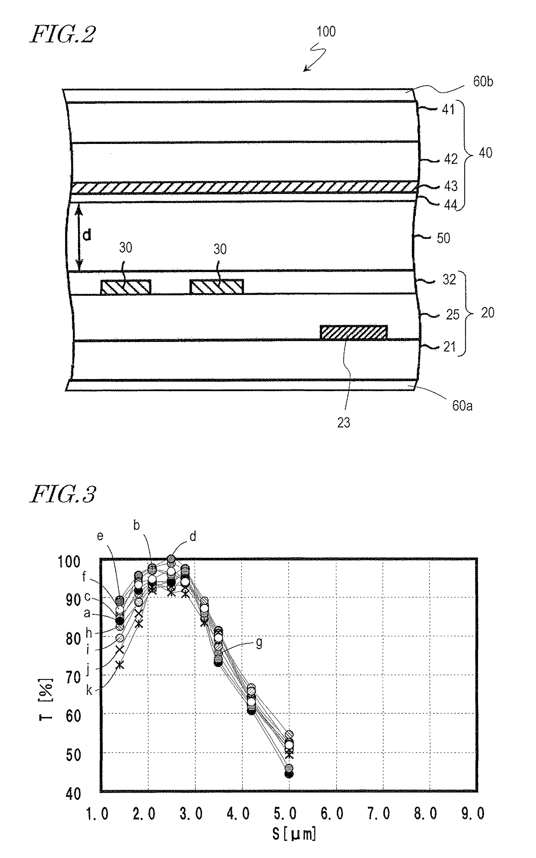
[0068]FIG. 1 is a plan view schematically showing a structure of one pixel of a liquid crystal display device 100 of embodiment 1 of the present invention. FIG. 2 is a schematic cross-sectional view of the liquid crystal display device 100 taken along line A-A′ of FIG. 1.

[0069]The liquid crystal display device 100 is a vertical alignment type liquid crystal display device which includes a plurality of pixels 10 having the structure shown in FIG. 1 and which performs display in a normally-black mode using the pixels 10 arranged in a matrix. The liquid crystal display device 100 further includes, as shown in FIG. 2, a TFT substrate 20 which is an active matrix substrate, a counter substrate 40 which is a color filter substrate, and a liquid crystal layer 50 disposed between these substrates. The liquid crystal layer 50 includes nematic liquid crystal which has negative dielectric constant anisotropy (Δ∈<0).

[0070]The outer side of the TFT substrate 20 (opposite to the liquid crystal la...

embodiment 2

[0111]Hereinafter, a liquid crystal display device embodiment 2 of the present invention is described. The liquid crystal display device of embodiment 2 is different from the liquid crystal display device of embodiment 1 in that the pixel electrode 30 of embodiment 1 is replaced by a pixel electrode of a different fishbone shape, and the other elements are the same as those of embodiment 1. Therefore, only the pixel electrode is described below.

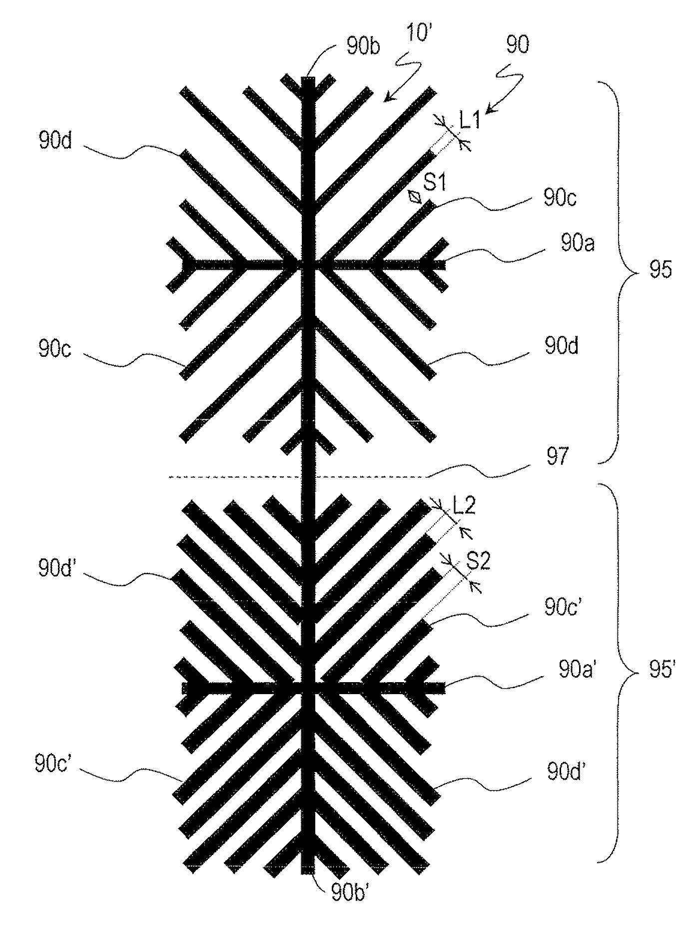
[0112]FIG. 9 is a plan view schematically showing the structure of a pixel electrode 90 in one of a plurality of pixels arranged in the liquid crystal display device of embodiment 2 (pixel 10′).

[0113]As shown in FIG. 9, the pixel electrode 90 includes trunk portions 90a and 90a′ extending in the direction of azimuthal angle 0°-180°, trunk portions 90b and 90b′ extending in the direction of azimuthal angle 90°-270°, a plurality of branch portions 90c and 90c′ (first branch portions) extending in the direction of azimuthal angle 45°-225° (first...


PUM

PropertyMeasurementUnit
widthaaaaaaaaaa
widthaaaaaaaaaa
widthaaaaaaaaaa

Abstract

There is provided a liquid crystal display device of high picture quality with high brightness and small display unevenness.A vertical alignment type liquid crystal display device which has a plurality of pixels includes: a first electrode which includes, in each of the plurality of pixels, a plurality of first branch portions extending in a first direction and a plurality of second branch portions extending in a second direction that is different from the first direction; a second electrode disposed so as to oppose the first electrode; and a liquid crystal layer interposed between the first electrode and the second electrode, wherein a width of each of the plurality of first branch portions and the plurality of second branch portions is in a range not less than 1.4 μm and not more than 8.0 μm.

Description

[0001]This application is the U.S. national phase of International Application No. PCT / JP2008 / 003722 filed 11 Dec. 2008 which designated the U.S. and claims priority to JP Patent Application No. 2007-340854 filed 28 Dec. 2007, the entire contents of each of which are hereby incorporated by reference.TECHNICAL FIELD[0002]The present invention relates to a liquid crystal display device and specifically to a vertical alignment type liquid crystal display device which has a plurality of divisional alignment regions in a pixel.BACKGROUND AND SUMMARY OF THE INVENTION[0003]As of now, liquid crystal display devices under development which have wide viewing angle characteristics includes liquid crystal display devices utilizing the IPS (In-Plane-Switching) mode which is a transverse electric field mode or the FFS (Fringe Field Switching) mode, and liquid crystal display devices utilizing the VA (Vertical Alignment) mode. The VA mode is better for mass production than the transverse electric ...

Claims


Application Information

Patent Timeline
Patent Type & Authority Patents(United States)
IPC IPC(8): G02F1/1337G02F1/1343
CPCG02F1/134309G02F1/133707G02F1/1393
Inventor OHGAMI, HIROYUKIHASHIMOTO, YOSHITOSHIBASAKI, MASAKAZUIYAMA, YUICHIKUBO, MASUMISOGA, MASAYUKI
Owner SHARP KK
Why Eureka
Try Eureka